
Switched capacitor integrator offset voltage elimination circuit and elimination method thereof

A technology of offset voltage and switched capacitors, applied in the direction of eliminating voltage/current interference, electronic switches, instruments, etc., can solve the problem of low precision of the integrator, achieve a wide range of applications, realize the effects of simple structure and low power consumption

Pending Publication Date: 2019-08-13
SHANGHAI FINGER TECH CO LTD
View PDF0 Cites 1 Cited by
  • Summary
  • Abstract
  • Description
  • Claims
  • Application Information

AI Technical Summary

Problems solved by technology

[0004] The invention provides a switched capacitor integrator offset voltage elimination circuit and its elimination method, for the first switch, the second switch, the third switch, the fourth switch, the first capacitor, the second capacitor, the third capacitor, the The four capacitors are reasonably set to keep the potential of point A unchanged during the integration and reset process, thereby eliminating the influence of the offset voltage on the integration, and solving the influence of the amplifier mismatch on the integrator in the switched capacitor integrator in the prior art, and the accuracy of the integrator low technical issues

Method used


Image

  • Switched capacitor integrator offset voltage elimination circuit and elimination method thereof
  • Switched capacitor integrator offset voltage elimination circuit and elimination method thereof
  • Switched capacitor integrator offset voltage elimination circuit and elimination method thereof

Examples


Embodiment 1

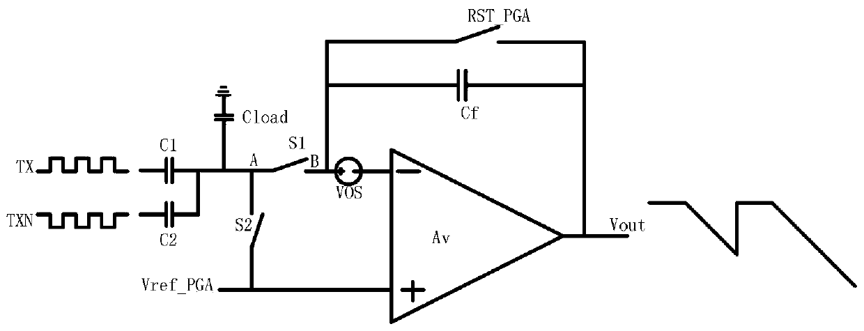
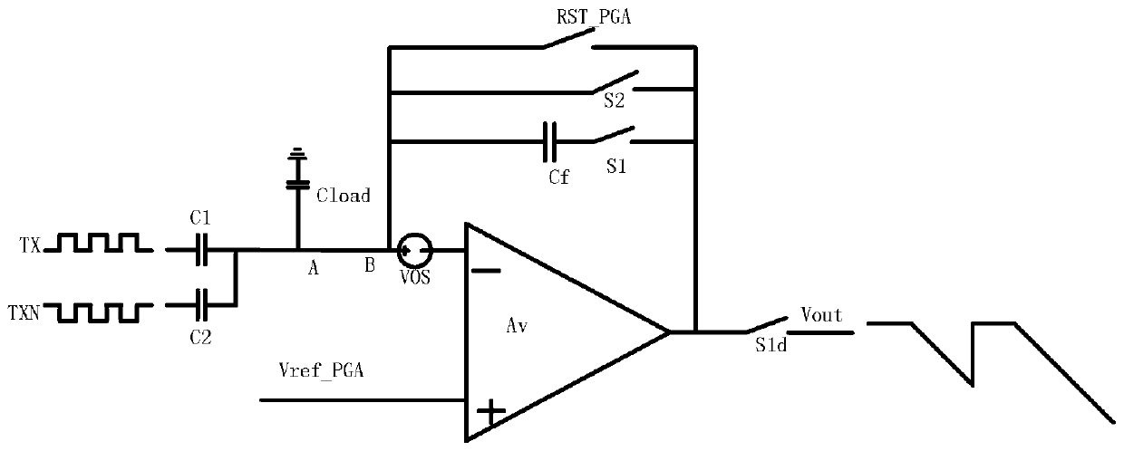
[0055] like figure 1 , figure 2 , image 3 As shown, a switched capacitor integrator offset voltage elimination circuit includes a first capacitor, a second capacitor, a third capacitor, a fourth capacitor, a first switch, a second switch, a third switch, a fourth switch, a reference voltage, VOS offset voltage source, integrator, one end of the first capacitor C1 is connected to the input signal, the second end is connected to the second end of the second capacitor C2, the first end of the third capacitor Cload, and the first end of the fourth capacitor Cf , the first end of the second switch S2, the first end of the third switch RST_PGA, and the first end of the VOS offset voltage source; one end of the first capacitor C2 is connected to the compensation signal, and the second end is connected to the second end of the first capacitor C1 Two terminals, the first terminal of the third capacitor Cload, the first terminal of the fourth capacitor Cf, the first terminal of the ...

Embodiment 2

[0082] A method for eliminating a switched capacitor integrator offset voltage eliminating circuit, comprising the following specific steps:

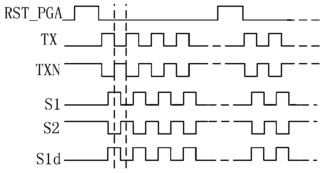
[0083] S100: Carry out overall reset through the switch, so that the integral circuit has an integral initial voltage;

[0084] S200: TX transmits continuous pulses, the integrator integrates on the falling edge of TX (the rising edge of TXN) through the switch control, and resets on the rising edge (the falling edge of TXN);

[0085] S300: In the process of integration and reset, keep the DC point of the input capacitor close to the operational amplifier unchanged, and there is an offset voltage of VOS at the DC point;

[0086] S400: Through correlated double sampling technology, two integral subtractions are performed to eliminate the DC point VOS offset voltage.

[0087] Wherein, in the step S200, TX transmits continuous pulses, the integrator is controlled by the second switch to integrate at the rising edge of TXN, and reset at the ...


PUM


Abstract

The invention discloses a switched capacitor integrator offset voltage elimination circuit and an elimination method thereof. The circuit comprises a first capacitor C1, a second capacitor C2, a thirdcapacitor Cload, a fourth capacitor Cf, a first switch S1, a second switch S2, a third switch RST _ PGA, a fourth switch S1d, a reference voltage Vref _ PGA, a VOS offset voltage source and an integrator. The first end of the first capacitor C1 is connected with an input signal, and the second end of the first capacitor C1 is connected with the second end of the second capacitor C2, the first endof the third capacitor Cload, the first end of the fourth capacitor Cf, the first end of the second switch S2, the first end of the third switch RST _ PGA and the first end of the VOS offset voltagesource. According to the technical scheme, the influence of a mismatched switched capacitor integrator is eliminated by optimizing a switch structure and a related double-sampling technology. The circuit is easy to implement, low in power consumption, capable of being used in a single-ended circuit and a differential circuit and wide in application range.

Description

technical field [0001] The invention relates to the technical field of fingerprint identification, in particular to a switched capacitor integrator offset voltage elimination circuit and an elimination method thereof. Background technique [0002] In consumer electronic products such as mobile phones and computers, in its key components, fingerprint recognition systems, capacitive fingerprint sensors with high integration are commonly used to realize fingerprint recognition. Due to the existence of valleys and ridges in the fingerprint texture, when the finger presses the mutual capacitance sensor array, when the electric field lines pass through the valleys and ridges, the magnitude of the mutual capacitance is also different because of the different media. Mutual-capacitance fingerprint sensors perform fingerprint recognition based on the difference in mutual capacitance between valleys and ridges. When a single transmit signal passes through the valley-ridge capacitance,...

Claims


Application Information

Patent Timeline
IPC IPC(8): H03K19/003H03K17/16H03K17/22H03K17/24G06K9/00
CPCH03K19/00346H03K17/168H03K17/22H03K17/24G06V40/1306
Inventor 徐汝云徐启波
Owner SHANGHAI FINGER TECH CO LTD
Features
  • Generate Ideas
  • Intellectual Property
  • Life Sciences
  • Materials
  • Tech Scout
  • Unparalleled Data Quality
  • Higher Quality Content
  • 60% Fewer Hallucinations
Learn More