Manufacturing method of MEMS bridge structure

A bridge structure and manufacturing method technology, applied in the field of MEMS bridge structure manufacturing, can solve problems such as bridge structure roll-up, and achieve the effect of preventing roll-up and collapse

Active Publication Date: 2019-08-16
SHANGHAI HUAHONG GRACE SEMICON MFG CORP
View PDF7 Cites 1 Cited by
  • Summary
  • Abstract
  • Description
  • Claims
  • Application Information

AI Technical Summary

Problems solved by technology

And because the amorphous silicon layer 102 and the electrode material layer 103 react easily, it will have adverse effects when removing the amorphous silicon layer 102, such as making the electrode material layer 103 roll up; in addition, the electrode material layer 103 inside itself There will also be stress problems that will cause the bridge structure to roll up

Method used


Image

  • Manufacturing method of MEMS bridge structure
  • Manufacturing method of MEMS bridge structure
  • Manufacturing method of MEMS bridge structure

Examples


Embodiment Construction

[0042] Such as figure 2 Shown is a flowchart of a method for manufacturing a MEMS bridge structure according to an embodiment of the present invention; Figure 3A to Figure 3J What is shown is a schematic diagram of the device structure in each step of the manufacturing method of the MEMS bridge structure in the embodiment of the present invention. The manufacturing method of the MEMS bridge structure in the embodiment of the present invention includes the following steps:

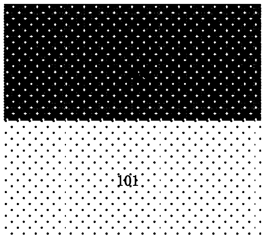
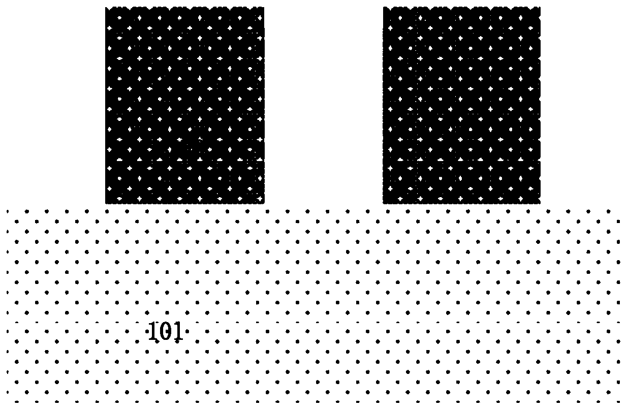
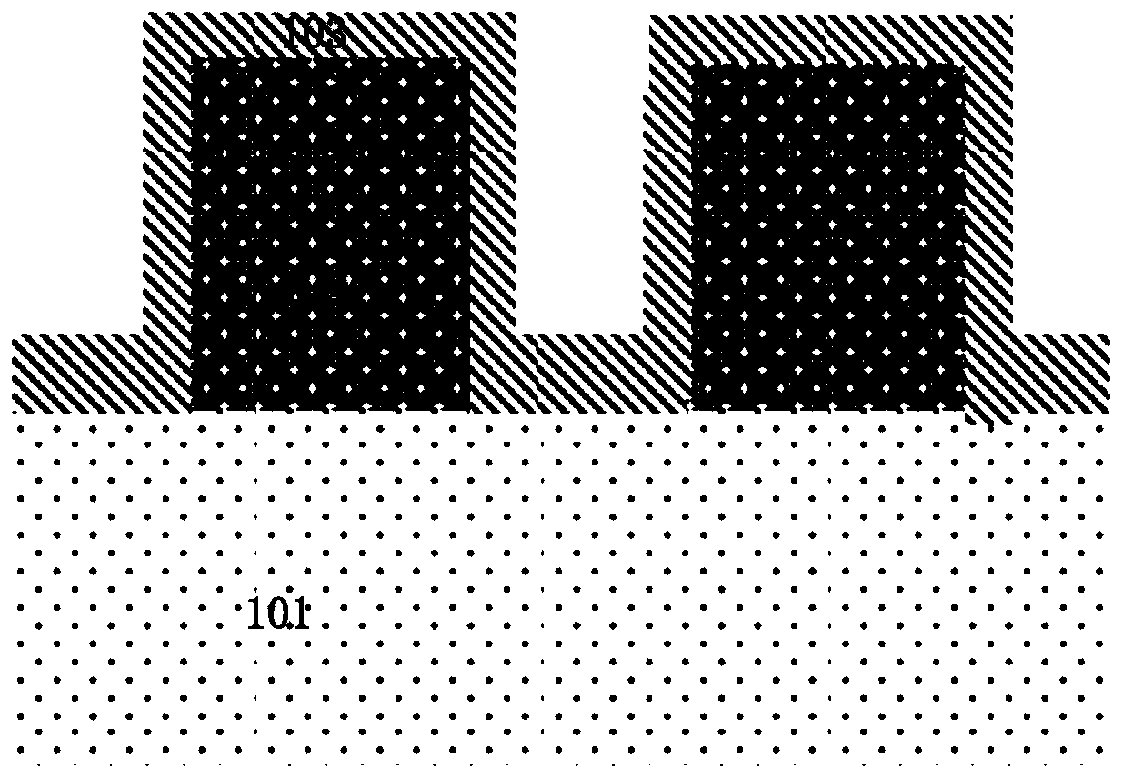
[0043] Step one, such as Figure 3A As shown, a substrate 1 is provided.

[0044] The substrate 1 is a silicon substrate 1. A device structure is formed on the substrate 1.

[0045] After that, like Figure 3B As shown, a first amorphous silicon layer 2 as a carrier is formed on the surface of the substrate 1.

[0046] The first amorphous silicon layer 2 is formed by a CVD process.

[0047] Step two, such as Figure 3B As shown, a first silicon dioxide layer 3 is formed on the surface of the first amorphous silico...


PUM


Abstract

The invention discloses a manufacturing method of an MEMS bridge structure. The manufacturing method comprises the steps of 1, forming a first amorphous silicon layer on the surface of a substrate; 2,forming a first silicon dioxide layer; 3, forming a bridge column hole; 4, forming a second silicon dioxide layer, wherein the surface of the first amorphous silicon layer is covered with the first silicon dioxide layer and the second silicon dioxide layer; 5, forming a second amorphous silicon layer serving as an induction thin film, and performing patterning; 6, etching to expose the surface ofthe substrate at the bottom of the bridge column hole; 7, forming an electrode material layer and patterning the electrode material layer, wherein the patterned electrode material layer is in contactwith the second amorphous silicon layer and the surface of the substrate; 8, forming an ONO layer and patterning the ONO layer, wherein the top of the electrode material layer is covered with patterned ONO layer to eliminate the stress; and 9, etching the first amorphous silicon layer to form a suspended bridge structure. According to the present invention, the bridge structure can be prevented from rolling upwards, and therefore the bridge structure can be prevented from collapsing.

Description

Technical field [0001] The invention relates to a semiconductor integrated circuit, in particular to a manufacturing method of a MEMS bridge structure. Background technique [0002] MEMS devices are widely concerned in the semiconductor industry, especially in sensors. The formation process of electrodes in MEMS devices is an important process step in existing MEMS devices, and MEMS electrodes play an extremely important role. In the existing process, amorphous silicon is used as the main carrier in the electrode of the MEMS device, and the electrode material is usually TiN film, that is, the TiN film is used as the connecting wire. However, when the metal of the electrode material is in direct contact with amorphous silicon, it is extremely easy to react between the metal and amorphous silicon; and in the MEMS bridge structure, it is necessary to remove the amorphous silicon as the carrier layer, so that the electrode is a suspended bridge Structure, and because the amorphous ...

Claims


Application Information

Patent Timeline
IPC IPC(8): B81C1/00
CPCB81C1/00349B81C1/00373B81C1/00404
Inventor 刘善善朱黎敏
Owner SHANGHAI HUAHONG GRACE SEMICON MFG CORP
Why Eureka
Try Eureka