Infrared absorption film and preparation method thereof

An infrared absorption and film technology, applied in the field of infrared absorption film and its preparation, can solve the problems of poor compatibility of micromachining process, expensive preparation equipment, etc., and achieve the effects of enhancing infrared absorption rate, increasing roughness, and improving overall performance

Active Publication Date: 2019-08-16
INST OF MICROELECTRONICS CHINESE ACAD OF SCI
View PDF4 Cites 2 Cited by
  • Summary
  • Abstract
  • Description
  • Claims
  • Application Information

AI Technical Summary

Problems solved by technology

[0004] In view of the above analysis, the present application aims to provide a method that solves the problems that the infrared absorbing film in the prior art only has high absorption capacity in a narrow short-wave range, the preparation equipment is expensive, and the compatibility of micro-processing technology is poor.

Method used


Image

  • Infrared absorption film and preparation method thereof
  • Infrared absorption film and preparation method thereof
  • Infrared absorption film and preparation method thereof

Examples


preparation example Construction

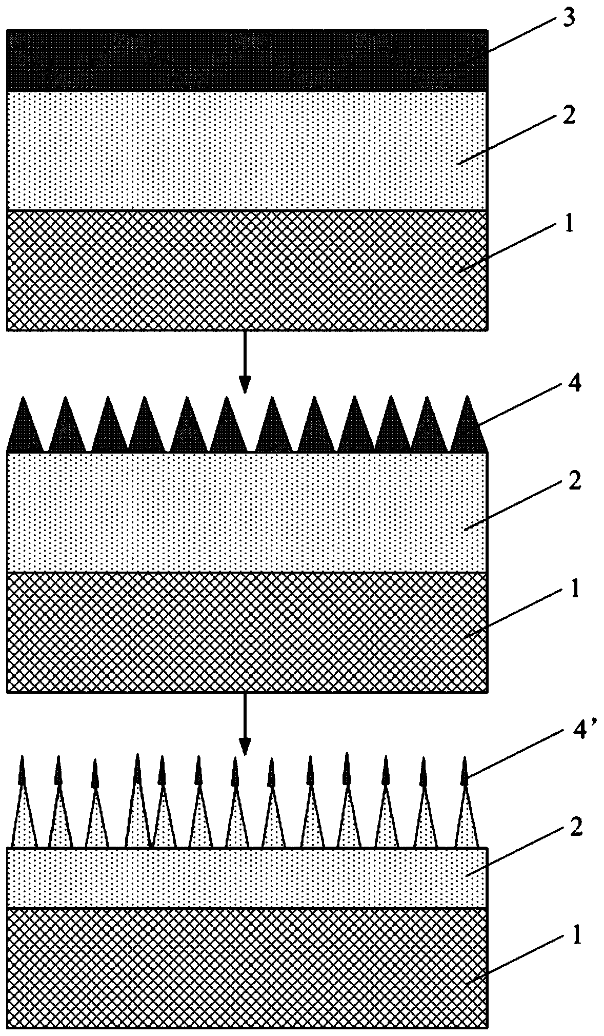
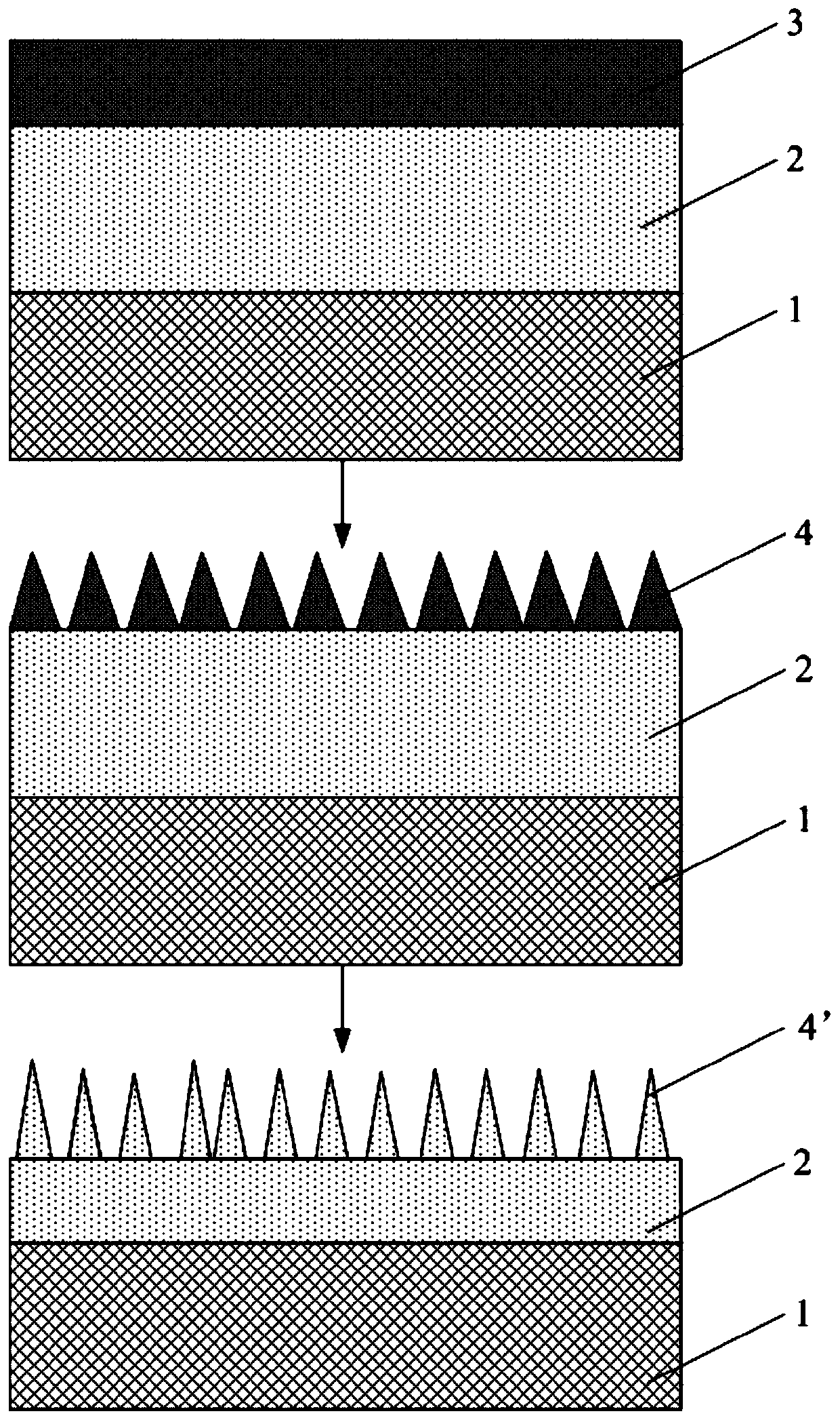
[0044] The application provides a method for preparing an infrared absorbing film, see Figure 1 to Figure 2 , including the following steps:

[0045] Form the sensitive layer 1 (for example, VO X layer or α-Si layer);

[0046] On the sensitive layer 1, an absorbing passivation layer 2 (for example, Si 3 N 4 layer) and graphic transfer layer 3;

[0047] Forming a nanostructure 4 on the side of the pattern transfer layer 3 away from the absorption passivation layer 2 by using the first plasma etching;

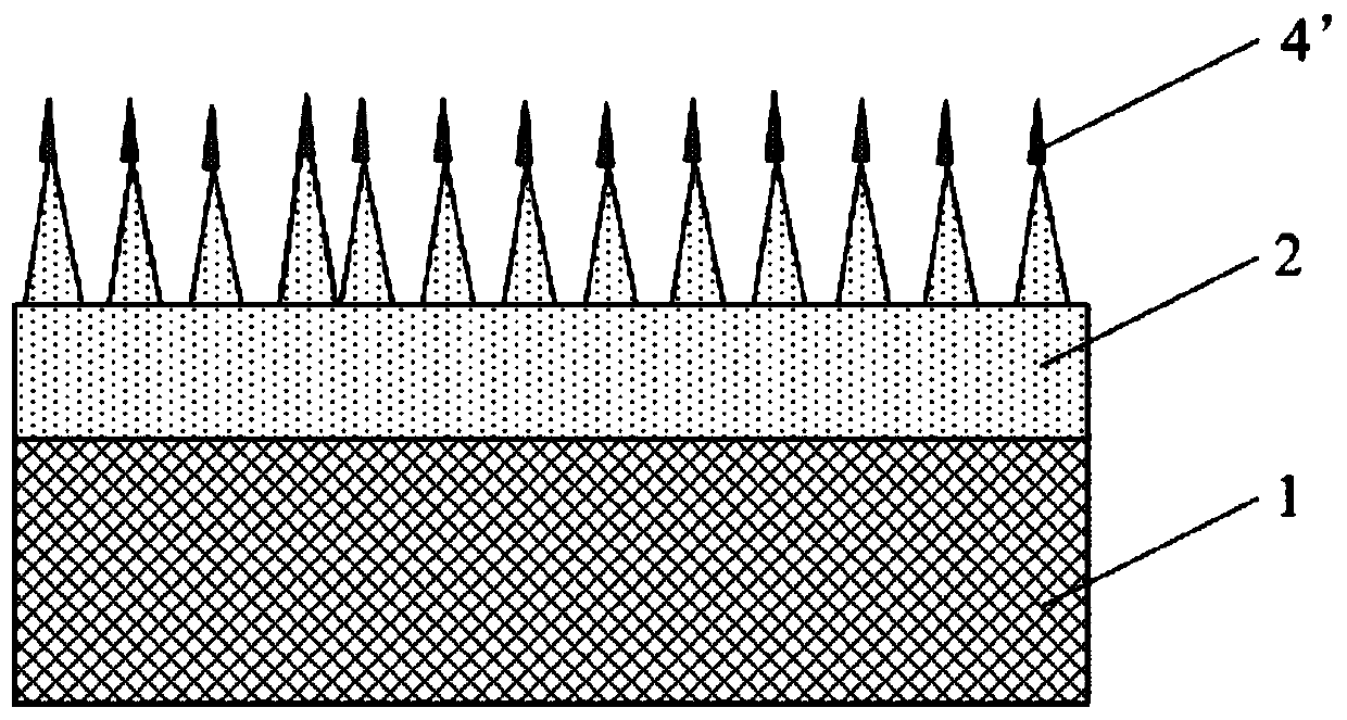
[0048] The nanostructure 4 of the pattern transfer layer 3 is transferred to the absorption passivation layer 2 by the second plasma etching, and the nanostructure 4' is formed on the side of the absorption passivation layer 2 away from the sensitive layer 1 to obtain an infrared absorption film.

[0049] It should be noted that the application of the preparation method of the infrared absorbing thin film of the present application is not limited to infrared absorption, and...

Embodiment 1

[0067] The preparation method of the infrared absorbing film of the present embodiment comprises the following steps:

[0068] form a sensitive layer;

[0069] An absorption passivation layer is formed on the sensitive layer, and a Ta layer is formed on the side of the absorption passivation layer away from the sensitive layer by using a magnetron sputtering process, as a pattern transfer layer, and the thickness of the pattern transfer layer is 100nm;

[0070] Utilize the first plasma etching to form a nanostructure on the side of the Ta layer away from the absorption passivation layer, wherein the etching conditions of the first plasma etching are as follows:

[0071] The etching gas pressure is 65mT, the upper radio frequency is 1600W, and the lower radio frequency is 40W. The etching gas includes C 4 f 6 , CO and Ar, C 4 f 6 The flow rate of CO is 10sccm, the flow rate of CO is 10sccm, and the flow rate of Ar is 250sccm;

[0072] Part or all of the Ta layer is etched ...

Embodiment 2

[0076] The preparation method of the infrared absorbing film of the present embodiment comprises the following steps:

[0077] form a sensitive layer;

[0078]Form an absorption passivation layer on the sensitive layer, and use ALD process to form a Ta layer on the side away from the sensitive layer of the absorption passivation layer, as a pattern transfer layer, and the thickness of the pattern transfer layer is 850nm;

[0079] Utilize the first plasma etching to form a nanostructure on the side of the Ta layer away from the absorption passivation layer, wherein the etching conditions of the first plasma etching are as follows:

[0080] The etching gas pressure is 297mT, the upper radio frequency is 3000W, and the lower radio frequency is 80W. The etching gas includes C 4 f 8 , CO and Ar, C 4 f 6 The flow rate of CO is 180sccm, the flow rate of CO is 185sccm, and the flow rate of Ar is 475sccm;

[0081] Part or all of the Ta layer is etched by the second plasma etching,...


PUM


Abstract

The invention discloses an infrared absorption film and a preparation method thereof, belongs to the technical field of microelectronic manufacturing, and solves the problems in the prior art that theinfrared absorption film has high absorption capacity only in a very narrow short-wave range, expensive preparation equipment and poor compatibility of micro-processing processes. The preparation method comprises the following steps: forming a sensitive layer; forming an absorption passivation layer and a pattern transfer layer on the sensitive layer in turn; forming a nanostructure on the side of the pattern transfer layer away from the absorption passivation layer by the first plasma etching; and transferring the nanostructure of the pattern transfer layer to the absorption passivation layer by the second plasma etching. The infrared absorption film comprises the sensitive layer and the absorption passivation layer which are laminated, wherein the nanostructure is formed on the side ofthe absorption passivation layer away from the sensitive layer. The infrared absorption film and the preparation method thereof can be used for infrared devices.

Description

technical field [0001] The application relates to a microelectronic manufacturing technology, in particular to an infrared absorbing film and a preparation method thereof. Background technique [0002] Infrared absorbing film is a key component that affects the infrared absorbing ability of infrared detectors. Black silicon and gold black are considered to be effective materials for improving the infrared absorbing ability of infrared detectors because of their special size effect and surface effect. [0003] However, limited by its silicon-based material properties, black silicon only has a high absorption capacity in a narrow short-wave range, making it difficult to meet the needs of long-wave detection of matter. Although the gold-black nanostructure can have high absorption capacity in a wide range of wavelengths, its preparation process is rigorous and complicated, requiring expensive equipment, and the obtained gold-black structure is fragile and has poor adhesion, whi...

Claims


Application Information

Patent Timeline
Patent Type & Authority Applications(China)
IPC IPC(8): H01L31/18H01L31/0216H01L31/0236
CPCH01L31/0216H01L31/02366H01L31/18Y02P70/50
Inventor 李俊杰傅剑宇高建峰周娜王桂磊李永亮杨涛李俊峰王文武
Owner INST OF MICROELECTRONICS CHINESE ACAD OF SCI
Why Eureka
Try Eureka