Supercharge Your Innovation With Domain-Expert AI Agents!

Method for patterning nanoparticle layer, quantum dot light-emitting device and display device

A quantum dot light-emitting, nano-particle technology, applied in nano-optics, chemical instruments and methods, luminescent materials, etc., can solve problems such as difficult to achieve, high resolution, and no breakthrough in QLED high-resolution patterning technology. Good performance, high-resolution effects

Active Publication Date: 2021-11-16
BOE TECH GRP CO LTD
View PDF11 Cites 0 Cited by
  • Summary
  • Abstract
  • Description
  • Claims
  • Application Information

AI Technical Summary

Problems solved by technology

However, the production efficiency of QLED has not yet reached the level of mass production. The most important reason is that the high-resolution patterning technology of QLED has not yet achieved a breakthrough.
[0003] Quantum dots are zero-dimensional nano-semiconductor materials. The size of the three dimensions of quantum dots is not greater than twice the exciton Bohr radius of the corresponding semiconductor material. When manufacturing patterned quantum dots in the prior art, due to the Due to the characteristics of inorganic nanoparticles, it is impossible to make patterned quantum dots by evaporation and patterning
[0004] In the prior art, patterned quantum dots are generally produced by inkjet printing, but it is difficult to achieve high resolution with this method
In order to improve the resolution of products in the prior art, photolithography is used to make patterned quantum dots. Since photolithography includes an exposure process, the exposure process is likely to affect the performance of quantum dots.
[0005] In summary, the existing technology cannot make a patterned high-resolution quantum dot layer
Similarly, inorganic nanoparticles with properties similar to quantum dots cannot form patterned high-resolution films according to existing technologies.

Method used


Image

  • Method for patterning nanoparticle layer, quantum dot light-emitting device and display device
  • Method for patterning nanoparticle layer, quantum dot light-emitting device and display device
  • Method for patterning nanoparticle layer, quantum dot light-emitting device and display device

Examples


Embodiment 1

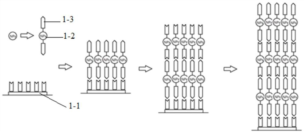
[0120] 1.1 Nanoparticle treatment

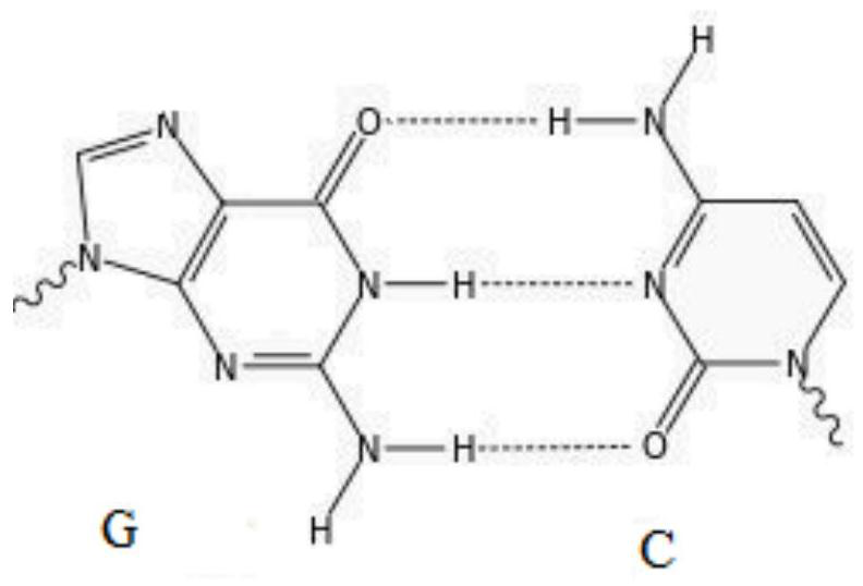
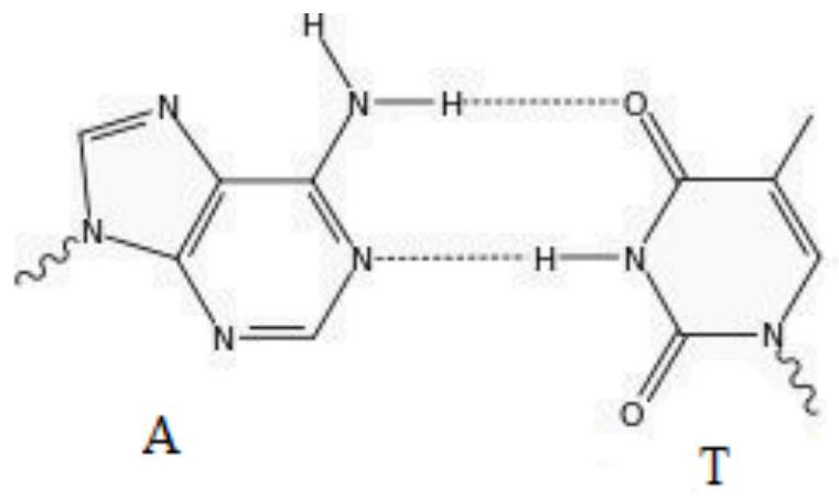
[0121] 1.1.1 Mix the ligand containing adenine (A) and the nanoparticle solution, precipitate after stirring, and centrifuge to obtain adenine-modified nanoparticles (A-NPs);

[0122] 1.1.2 The ligand containing thymine (T) and the nanoparticle solution were mixed, stirred, precipitated, and centrifuged to obtain thymine-modified nanoparticles (T-NPs).

[0123] 1.2 Nanoparticle deposition

[0124] 1.2.1 Chemically modify the substrate to obtain a substrate containing T on the surface; specifically:

[0125]1) Hydroxylation of the substrate: soak the glass substrate in the mixed washing solution of concentrated sulfuric acid and hydrogen peroxide (the volume ratio of concentrated sulfuric acid: hydrogen peroxide is 7:3), heat it to 80 degrees Celsius for 5 hours, and wash it with deionized water after the reaction , to obtain a hydroxylated glass substrate; 2) chemical modification: soak the substrate in a toluene solution (0.5mmol / L) conta...

Embodiment 2

[0131] 2.1 Quantum dot processing

[0132] According to the scheme of 1.1.1, quantum dots 1, 2, and 3 were modified with ligands containing A, T, G, C, X, and Y bases, respectively, to obtain corresponding quantum dots A-NPs 1, T-NPs 1, G-NPs 2, C-NPs 2, X-NPs 3, Y-NPs 3.

[0133] 2.2 Substrate processing and deposition

[0134] 2.2.1 Use methods such as printing, transfer printing, and exposure to modify different preset regions of the substrate with bases containing T, C, and Y;

[0135] 2.2.2 Coating A-NPs on the modified substrate, and forming an A-NPs quantum dot layer in the T-modified preset area after assembly;

[0136] 2.2.3 Coating T-NPs on the substrate, the surface of A-NPs will continue to deposit T-NPs;

[0137] 2.2.4 Repeat the two steps 2.2.2 and 2.2.3 to form a NPs 1 quantum dot layer in the preset area modified by T, and no quantum dots are deposited in the positions modified by C and Y;

[0138] 2.2.5 Alternately coat G-NPs 2, C-NPs 2, X-NPs 3, and Y-NPs...

Embodiment 3

[0140] 3.1 Quantum dot processing

[0141] 3.1.1 Mix the ligand containing adenine (A) and the quantum dot solution, precipitate after stirring, and centrifuge to obtain adenine-modified quantum dots (A-NPs);

[0142] 3.1.2 Mix the ligand containing thymine (T) and the quantum dot solution, stir, precipitate, and centrifuge to obtain thymine-modified quantum dots (T-NPs).

[0143] 3.2 Substrate processing and deposition

[0144] 3.2.1 Coat zinc oxide quantum dots on the Qled substrate containing the pixel structure, anneal at 30mg / mL, 2000rpm, and 100°C for 30 minutes to obtain a zinc oxide film.

[0145] Print a solution (0.5mmol / L) containing 1H, 1H, 2H, 2H-perfluorododecyltrichlorosilane in the desired pixel, let it stand for 10 minutes, and rinse with toluene to obtain a C8F17 group containing the substrate.

[0146] The compound containing the base T and C8F17 group was dissolved in the solution (1 mg / mL), and the substrate was immersed in it at room temperature for 10...


PUM


Abstract

The invention relates to the display field, in particular to a method for patterning a nano particle layer, a quantum dot light-emitting device and a display device. The method for patterning the nanoparticle layer of the present invention includes the following steps: (S1) connecting the first base to the surface of the preset region of the substrate to form a substrate modified with the first base; (S2) attaching the first base to the surface of the substrate Depositing nanoparticles in the predetermined area, the ligand of the nanoparticles contains a second base, the first base and the second base are connected by hydrogen bonds, self-assembled to form a nanoparticle layer; (S3) removing Nanoparticles not involved in hydrogen bonding. The present invention can complete the patterning of the nanoparticle layer, especially the quantum dot layer, without using an inkjet printing method or a photolithography method, and can form a nanoparticle layer with high resolution and good performance.

Description

technical field [0001] The invention relates to the display field, in particular to a method for patterning a nano particle layer, a quantum dot light-emitting device and a display device. Background technique [0002] With the in-depth development of quantum dot preparation technology, the stability and luminous efficiency of quantum dots continue to improve, and the research on quantum dot electroluminescent diodes (Quantum Light Emitting Diode, QLED) continues to deepen, and the application prospects of QLED in the display field are increasingly bright. However, the production efficiency of QLED has not yet reached the level of mass production. The most important reason is that the high-resolution patterning technology of QLED has not yet achieved a breakthrough. [0003] Quantum dots are zero-dimensional nano-semiconductor materials. The size of the three dimensions of quantum dots is not greater than twice the exciton Bohr radius of the corresponding semiconductor mater...

Claims


Application Information

Patent Timeline
Patent Type & Authority Patents(China)
IPC IPC(8): H01L51/56H01L51/50H01L27/32
CPCH10K50/115C09K11/06B82Y20/00B82Y40/00H10K59/35H10K71/13H10K71/236B82Y30/00C09K2211/1048C09K2211/1074H10K50/15H10K50/16H10K71/00
Inventor 张振琦
Owner BOE TECH GRP CO LTD
Features
  • R&D
  • Intellectual Property
  • Life Sciences
  • Materials
  • Tech Scout
  • Unparalleled Data Quality
  • Higher Quality Content
  • 60% Fewer Hallucinations
Learn More