Method of driving flexible photonic crystal to change color based on shape memory alloy polymer
A technology of memory alloy and photonic crystal, which is applied in optics, optical components, instruments, etc., can solve the problems of insufficient flexibility of the overall structure of photonic crystal discoloration and high driving voltage, so as to achieve precise control and stable display, ensure stretchability, Solve the effect of insufficient flexibility
- Summary
- Abstract
- Description
- Claims
- Application Information
AI Technical Summary
Problems solved by technology
Method used
Image
Examples
preparation example Construction
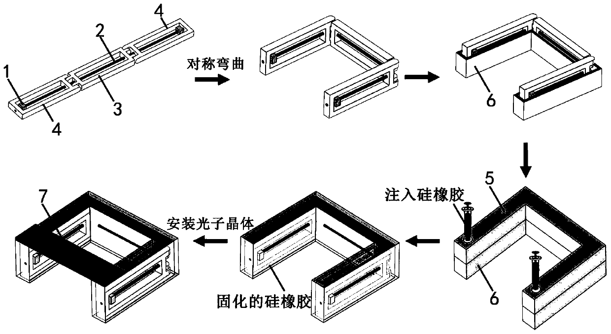
[0044] S2. Preparation of flexible photonic crystals;
[0045] S201. Process a cylinder array on the silicon wafer by ion beam processing, wherein the diameter of the cylinders is 200-600nm, the depth is 200-600nm, the hole spacing is 400-1200nm, and the arrangement is a triangular arrangement;
[0046] S202. Pouring Dow Corning 184 silicone rubber on the surface of the processed silicon wafer and heating at 40-80° C. for 2-6 hours to solidify, so as to prepare a flexible photonic crystal.
[0047] S3, preparation of the overall discoloration structure;
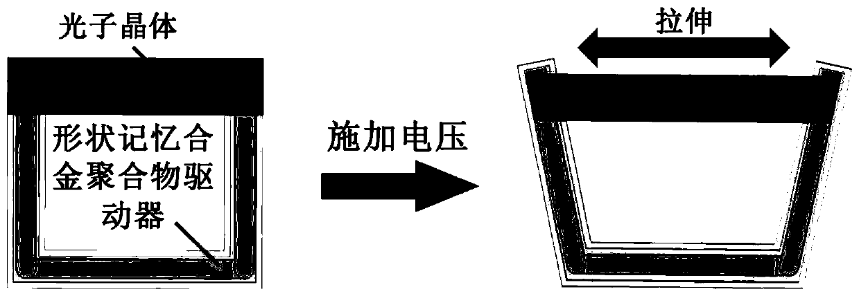
[0048] The flexible photonic crystal is connected with the U-shaped actuator based on shape memory alloy polymer through Smooth-on silicone rubber adhesive.
[0049] S4, discoloration process;
[0050] S401. First fix the bottom of the U-shaped driver stably, adjust the intensity and position of the light source, so that the surface of the photonic crystal appears red;
[0051] Wherein, the light source is a 5-40W white li...
Embodiment 1
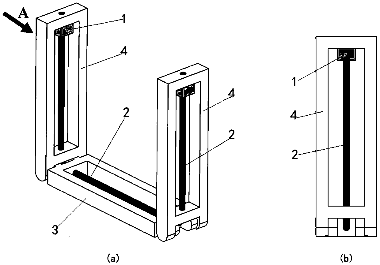
[0060] 1) Preparation of the driver;
[0061] A shape memory alloy wire with a diameter of 1 mm is inserted into the designed rigid structure to form a U-shaped driving structure. Further, Ecoflex-0050 silicone rubber is poured on its surface and heated at 40°C for 3 hours to cure, forming a U-shaped driver based on a shape memory alloy polymer;
[0062] 2) Preparation of flexible photonic crystals;
[0063] A cylindrical array is processed on a silicon wafer by ion beam processing, in which the diameter of the cylinder is 400nm, the depth is 400nm, the hole spacing is 800nm, and the arrangement is triangular; Dow Corning 184 silicone rubber is poured on the surface of the processed silicon wafer and heated at 60°C for 4 Hours of curing, the preparation of flexible photonic crystals;
[0064] 3) Preparation of the overall color-changing structure;
[0065] The flexible photonic crystal is connected to the U-shaped driver based on the shape memory alloy polymer through the S...
Embodiment 2
[0071] 1) Preparation of the driver;
[0072] A shape memory alloy wire with a diameter of 0.4 mm is inserted into the designed rigid structure to form a U-shaped driving structure. Further, Ecoflex-0050 silicone rubber is poured on its surface and heated at 20°C for 6 hours to cure, forming a U-shaped driver based on a shape memory alloy polymer;
[0073] 2) Preparation of flexible photonic crystals;
[0074] Process a cylindrical array on a silicon wafer by ion beam processing, in which the diameter of the cylinder is 200nm, the depth is 200nm, the hole spacing is 400nm, and the arrangement is triangular arrangement; Dow Corning 184 silicone rubber is poured on the surface of the processed silicon wafer and heated at 40°C for 6 Hours of curing, the preparation of flexible photonic crystals;
[0075] 3) Preparation of the overall color-changing structure;
[0076] The flexible photonic crystal is connected to the U-shaped driver based on the shape memory alloy polymer thro...
PUM
| Property | Measurement | Unit |
|---|---|---|
| Diameter | aaaaa | aaaaa |
| Diameter | aaaaa | aaaaa |
| Depth | aaaaa | aaaaa |
Abstract
Description
Claims
Application Information


