Method for preparing epitaxial wafer of light-emitting diode and epitaxial wafer

A technology of light-emitting diodes and epitaxial wafers, applied in the preparation of epitaxial wafers, in the field of epitaxial wafers, can solve the problems of unsatisfactory crystal quality and influence of epitaxial wafers, and achieve the effects of promoting diffusion and migration, improving quality, and improving crystal quality

Active Publication Date: 2019-08-20
HC SEMITEK CORP
View PDF5 Cites 8 Cited by
  • Summary
  • Abstract
  • Description
  • Claims
  • Application Information

AI Technical Summary

Problems solved by technology

[0003] The AlN buffer layer between the substrate and the non-doped GaN layer can reduce the lattice mismatch between the substrate and the non-doped GaN layer, but the quality of the AlN buffer layer directly grown on the substrate is still There are certain defects, which affect the quality of the non-doped GaN layer, N-type GaN layer, multi-quantum well layer and P-type GaN layer grown on the AlN buffer layer, resulting in the crystal quality of the final epitaxial wafer is still not ideal

Method used


Image

  • Method for preparing epitaxial wafer of light-emitting diode and epitaxial wafer
  • Method for preparing epitaxial wafer of light-emitting diode and epitaxial wafer
  • Method for preparing epitaxial wafer of light-emitting diode and epitaxial wafer

Examples


Embodiment Construction

[0032] In order to make the object, technical solution and advantages of the present invention clearer, the implementation manner of the present invention will be further described in detail below in conjunction with the accompanying drawings.

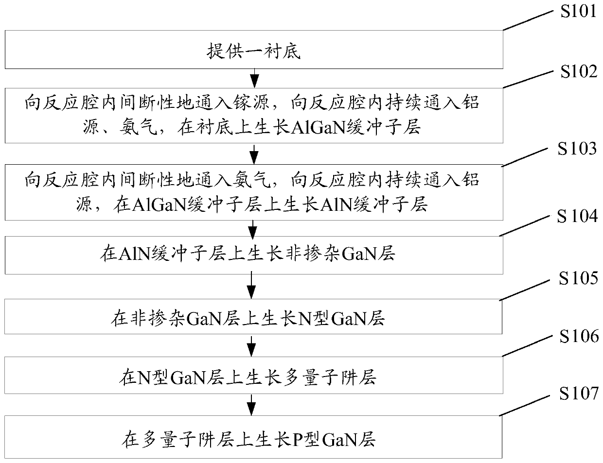
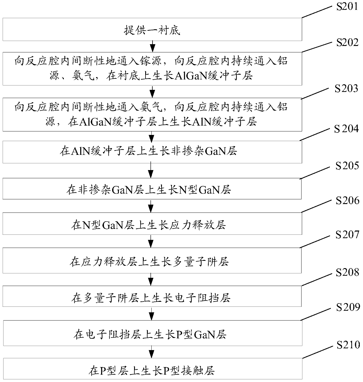
[0033] figure 1 It is a flow chart of a method for preparing an epitaxial wafer of a light-emitting diode provided by an embodiment of the present invention, such as figure 1 Shown, this preparation method comprises:

[0034] S101: Provide a substrate.

[0035] S102: intermittently injecting a gallium source into the reaction chamber, continuously injecting an aluminum source and ammonia into the reaction chamber, and growing an AlGaN buffer sublayer on the substrate.

[0036] S103: intermittently inject ammonia gas into the reaction chamber, continuously inject aluminum source into the reaction chamber, and grow an AlN buffer sublayer on the AlGaN buffer sublayer.

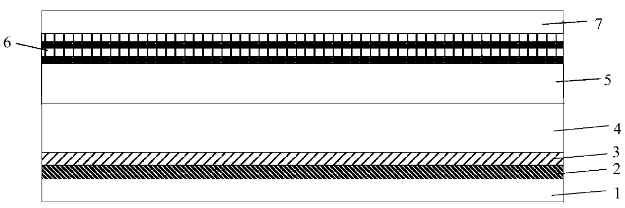
[0037] S104: growing a non-doped GaN layer on the AlN buffer subla...


PUM


Abstract

The invention discloses a method for preparing an epitaxial wafer of a light-emitting diode and the epitaxial wafer and belongs to the field of light-emitting diode fabrication. A gallium source is intermittently introduced into a reaction chamber and an aluminum source is continuously introduced into the reaction chamber, the intermittent introduction of the gallium source allows an appropriate amount of gallium atoms to exist in the reaction chamber, the appropriate amount of gallium atoms act as an activator, the quality of an obtained AlGaN buffer sub layer is good, a AlN buffer sub layeris welled matched with the AlGaN buffer sub layer with appropriate amount of gallium atoms, and the quality of the AlN buffer sub layer grown on the AlGaN buffer sub layer is improved. When the AlN buffer sub layer is grown, due to the gas phase reaction between an ammonia gas and the aluminum source, a part of the reactants generated by the reaction are incorporated into the AlN buffer sub layer,and the quality of the AlN buffer sub layer is affected. The ammonia gas is intermittently introduced, the reduction of the ammonia gas can inhibit the gas phase reaction between aluminum and the ammonia gas, a reactant of the ammonia gas and aluminum source reaction growth is reduced and is combined into the AlN buffer sub layer, and finally the crystal quality of the epitaxial wafer is improved.

Description

technical field [0001] The invention relates to the field of light-emitting diode production, in particular to a method for preparing an epitaxial wafer of a light-emitting diode and the epitaxial wafer. Background technique [0002] The epitaxial wafer is the basic structure for making light-emitting diodes. The structure of the epitaxial wafer includes a substrate and an epitaxial layer grown on the substrate. Among them, the structure of the epitaxial layer mainly includes: an AlN buffer layer, a non-doped GaN layer, an N-type GaN layer, a multi-quantum well layer and a P-type GaN layer grown sequentially on the substrate. [0003] The AlN buffer layer between the substrate and the non-doped GaN layer can reduce the lattice mismatch between the substrate and the non-doped GaN layer, but the quality of the AlN buffer layer directly grown on the substrate is still There are certain defects, which affect the quality of the non-doped GaN layer, N-type GaN layer, multi-quantu...

Claims


Application Information

Patent Timeline
Patent Type & Authority Applications(China)
IPC IPC(8): H01L33/00H01L33/06H01L33/12
CPCH01L33/007H01L33/06H01L33/12
Inventor 蒋媛媛纪磊从颖胡加辉李鹏
Owner HC SEMITEK CORP
Why Eureka
Try Eureka