Group iii-nitride semiconductor substrate, and method for manufacturing group iii-nitride semiconductor substrate
A technology of nitride semiconductors and manufacturing methods, which is applied in semiconductor/solid-state device manufacturing, semiconductor devices, chemical instruments and methods, etc., and can solve the problems of internal quantum efficiency reduction and other issues
- Summary
- Abstract
- Description
- Claims
- Application Information
AI Technical Summary
Problems solved by technology
Method used
Image

Examples
no. 1 approach >
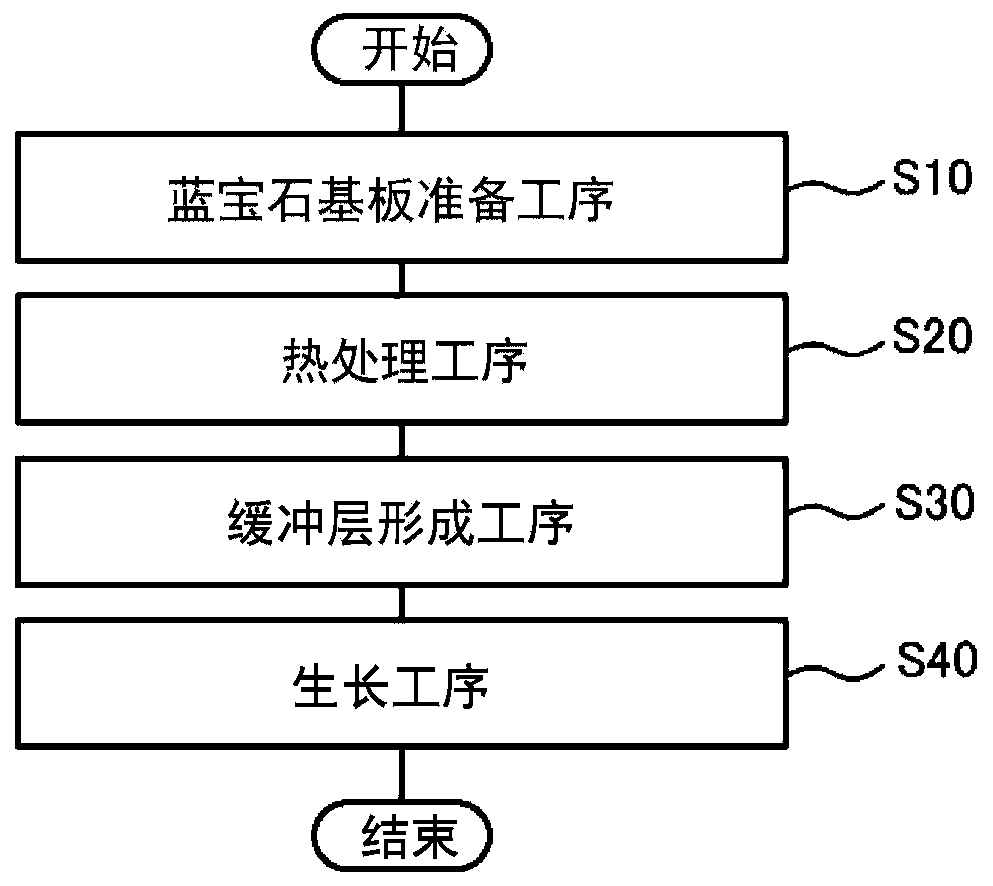
[0032] First, an example of a method for manufacturing a group III nitride semiconductor substrate according to this embodiment will be described. figure 1 It is a flowchart showing an example of the process flow of the method for manufacturing a group III nitride semiconductor substrate according to the present embodiment. As shown in the figure, the method for manufacturing a group III nitride semiconductor substrate according to this embodiment includes a sapphire substrate preparation step S10 , a heat treatment step S20 , a buffer layer forming step S30 , and a growth step S40 .
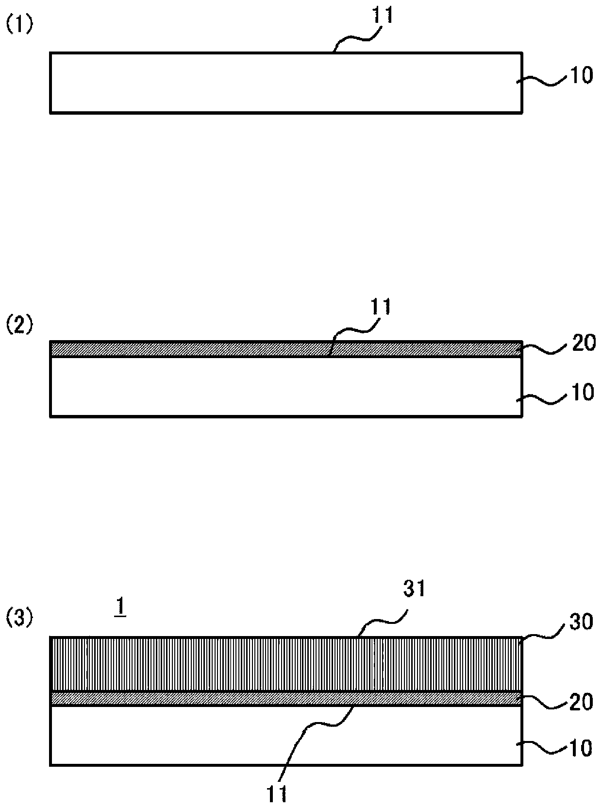
[0033] In the sapphire substrate preparation step S10 , a sapphire substrate having a {10-10} plane or a {10-10} plane as a main surface inclined at a predetermined angle in a predetermined direction is prepared. figure 2 (1) shows an example of a schematic side view of the sapphire substrate 10 prepared in this step. The diameter of the sapphire substrate 10 is, for example, 1 inch or more. ...
no. 1 example >
[0138] Various sapphire substrates 10 are prepared for the plane orientation (first factor) of the plurality of main surfaces 11 . The sapphire substrate 10 has a thickness of 430 μm and a diameter of 2 inches.
[0139] Next, each prepared sapphire substrate 10 was heat-treated under the following conditions.
[0140] Temperature: 950℃~1100℃.
[0141] Pressure: 200torr.
[0142] Heat treatment time: 10 minutes or 15 minutes.
[0143] Carrier gas: H 2 , N 2 .
[0144] h 2 (Carrier gas) supply volume: 4.0slm~9.0slm.
[0145] N 2 (Carrier gas) supply volume: 1.5slm.
[0146] In addition, samples were produced in which the presence or absence (second factor) of nitriding treatment during heat treatment was different. Specifically, two types of samples were produced: NH 3 Samples subjected to nitriding treatment and NH not supplied during heat treatment 3 Samples without nitriding treatment.
[0147] After the heat treatment, a buffer layer 20 (AlN buffer layer) having...
no. 2 approach >
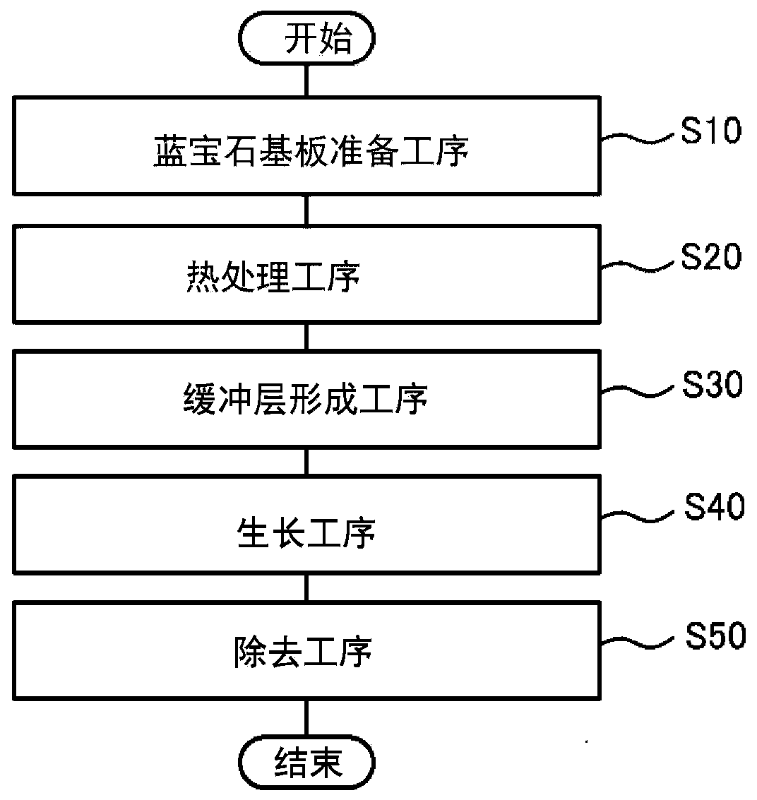
[0184] Figure 5 It is a flowchart showing an example of the process flow of the method for manufacturing a group III nitride semiconductor substrate according to the present embodiment. As shown in the figure, the method for manufacturing a III-nitride semiconductor substrate according to this embodiment includes a sapphire substrate preparation step S10, a heat treatment step S20, a preflow step S25, a buffer layer formation step S30, and a growth step S40. A removal step S50 may also be included. According to the present embodiment, the group III nitride semiconductor layer 30 can be formed by epitaxially growing the group III nitride semiconductor with the desired semipolar plane on the N polarity side as the growth plane. Next, each step will be described.
[0185] The sapphire substrate preparation step S10 is the same as that of the first embodiment.
[0186]In the heat treatment step S20 , the sapphire substrate 10 is heat-treated while performing the nitriding trea...
PUM
| Property | Measurement | Unit |
|---|---|---|
| thickness | aaaaa | aaaaa |
| thickness | aaaaa | aaaaa |
| thickness | aaaaa | aaaaa |
Abstract
Description
Claims
Application Information
 - R&D
- Intellectual Property
- Life Sciences
- Materials
- Tech Scout
- Unparalleled Data Quality
- Higher Quality Content
- 60% Fewer Hallucinations
Browse by: Latest US Patents, China's latest patents, Technical Efficacy Thesaurus, Application Domain, Technology Topic, Popular Technical Reports.
© 2025 PatSnap. All rights reserved.Legal|Privacy policy|Modern Slavery Act Transparency Statement|Sitemap|About US| Contact US: help@patsnap.com