MoS2-based thin-layer ultraviolet light-emitting diode and manufacturing method thereof

A light-emitting diode, thin-layer technology, applied in nanotechnology, electrical components, nanotechnology, etc. for materials and surface science, which can solve multiple threading dislocations, poor quality of n-AlGaN, limiting GaN-based deep ultraviolet LEDs development and other issues to achieve the effect of high crystal quality

Inactive Publication Date: 2020-05-12
江苏晶曌半导体有限公司
View PDF10 Cites 0 Cited by
  • Summary
  • Abstract
  • Description
  • Claims
  • Application Information

AI Technical Summary

Problems solved by technology

However, as the Al composition of AlGaN material increases, the difficulty of material epitaxy will also increase, and AlN single crystal substrates with high Al composition lattice matching are extremely expensive
In order to solve this problem, the usual practice is to grow a thick AlN buffer layer by two-step growth method before growing luminescent multiple quantum wells, and then grow n-AlGaN, but the n-AlGaN grown in this way has very Many threading dislocations, and the quality of n-AlGaN is very poor in the deep ultraviolet range
In addition, in order to isolate the impact of threading dislocations in the lower layer relative to the luminescent quantum well, the n-AlGaN layer is generally grown thicker, which also limits the development of GaN-based deep ultraviolet LEDs on flexible substrates and biological substrates.

Method used


Image

  • MoS2-based thin-layer ultraviolet light-emitting diode and manufacturing method thereof
  • MoS2-based thin-layer ultraviolet light-emitting diode and manufacturing method thereof
  • MoS2-based thin-layer ultraviolet light-emitting diode and manufacturing method thereof

Examples


preparation example Construction

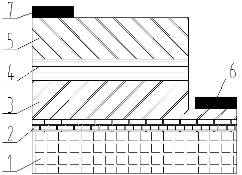
[0036] The invention also provides a MoS-based 2 The preparation method of the thin-layer ultraviolet light emitting diode includes the following steps:

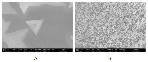
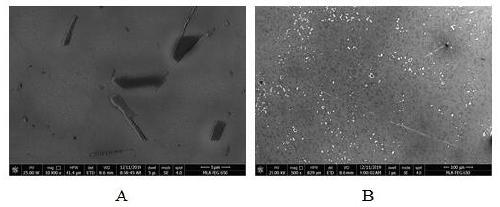
[0037] (1) On the substrate, use CVD process to grow MoS with a thickness of 2-5nm 2 The process conditions are: the temperature of the reaction chamber is 650-850°C, the pressure of the reaction chamber is maintained at 20-75 Torr, and nitrogen gas with a flow rate of 250-300sccm is introduced into the reaction chamber at the same time, and a drop of reduced graphene oxide solution is suspended before growth On the substrate surface of the substrate, then dry at 50 ℃, the MO 3 Put the powder into the CVD ceramic boat, and install the substrate face down on the top of the boat, and place the ceramic boat with a separate sulfur powder on the MO 3 Next to the powder.

[0038] (2) MoS covered with substrate 2 On the layer, use the MOCVD process to grow an n-type graded Al composition AlGaN layer with a thickness of 100-120nm by linea...

Embodiment 1

[0048] Embodiment 1. The preparation of a MoS2 thin-layer ultraviolet light emitting diode with a luminous wavelength of 320nm on a c-plane sapphire substrate includes the following steps:

[0049] Step 1: Pre-treat the substrate

[0050] After cleaning the c-plane sapphire substrate, it is placed in a chemical vapor deposition CVD reaction chamber, and the vacuum degree of the reaction chamber is reduced to 1×10 -1 Torr: Pour hydrogen into the reaction chamber, and when the pressure in the CVD reaction chamber reaches 200 Torr, heat the substrate to a temperature of 800°C and keep it for 15 minutes to complete the heat treatment of the substrate substrate;

[0051] Step two, grow MoS 2 Floor

[0052] On the treated substrate, a drop of reduced graphene oxide solution was suspended on the surface of the substrate substrate, and then dried at 50 ℃, the MO 3 The powder is placed in a CVD ceramic boat, and the substrate is mounted on the top of the boat with the substrate face down. Plac...

Embodiment 2

[0062] Example 2. Preparation of MoS with 295nm emission wavelength on c-plane sapphire substrate 2 The thin-layer ultraviolet light emitting diode includes the following steps:

[0063] Step 1: Pre-treat the substrate

[0064] After cleaning the c-plane sapphire substrate, it is placed in a chemical vapor deposition CVD reaction chamber, and the vacuum degree of the reaction chamber is reduced to 1×10 -1 Torr: Pour hydrogen into the reaction chamber, and when the pressure in the CVD reaction chamber reaches 200 Torr, heat the substrate to a temperature of 800° C. and keep it for 15 minutes to complete the heat treatment of the substrate substrate.

[0065] Step two, grow MoS 2 Floor

[0066] On the treated substrate, a drop of reduced graphene oxide solution was suspended on the surface of the substrate substrate, and then dried at 50 ℃, the MO 3 The powder is placed in a CVD ceramic boat, and the substrate is mounted on the top of the boat with the substrate face down. Place a separ...


PUM

PropertyMeasurementUnit
thicknessaaaaaaaaaa
thicknessaaaaaaaaaa
thicknessaaaaaaaaaa

Abstract

The invention provides a MoS2-based thin-layer ultraviolet light-emitting diode and a preparation method thereof. The MoS2-based thin-layer ultraviolet light-emitting diode comprises a substrate, an MoS2 layer, an n-type gradient Al component AlGaN layer, an AlGaN quantum well layer, a p-type gradient Al component AlGaN layer and a p electrode which are sequentially arranged from bottom to top; ann electrode is arranged on the lateral upper portion of the n-type gradient Al component AlGaN layer, and the MoS2 layer is made of a multilayer tiled MoS2 material. According to the invention, no dangling bond exists on the heteroepitaxy surface of MoS2, and the crystal quality is high. The epitaxial mode of the invention is Van der Waals epitaxy, and epitaxial growth can be realized on varioussubstrates. The MoS2-based thin-layer ultraviolet light-emitting diode is smaller in overall thickness and wide in application field.

Description

Technical field [0001] The invention relates to an ultraviolet light-emitting diode, in particular to a MoS-based 2 Thin-layer ultraviolet light-emitting diode and manufacturing method thereof. Background technique [0002] In the prior art, AlGaN ternary materials can be formed by doping Al in GaN, and by changing the Al composition in the quantum well, the band gap of AlGaN can be continuously changed within the range of 3.4eV~6.2eV. The working wavelength of the light emitting diode can be changed from 365nm to 200nm. However, with the increase of the Al composition of AlGaN materials, the difficulty of material epitaxy will also increase, and the price of AlN single crystal substrates that match the high Al composition lattice is extremely expensive. In order to solve this problem, the usual method is to grow a thick AlN buffer layer by a two-step growth method before growing the light-emitting multiple quantum well, and then grow n-AlGaN, but the n-AlGaN grown in this way h...

Claims


Application Information

Patent Timeline
Patent Type & Authority Applications(China)
IPC IPC(8): H01L33/12H01L33/02H01L33/14H01L33/00B82Y30/00B82Y40/00
CPCB82Y30/00B82Y40/00H01L33/007H01L33/025H01L33/12H01L33/14
Inventor 岳文凯白俊春平加峰
Owner 江苏晶曌半导体有限公司
Why Eureka
Try Eureka