Structure of antimonide quantum well CMOS device and preparation method thereof

An antimonide and quantum well technology, applied in the field of microelectronics, can solve the problems of increasing the difficulty of epitaxial material growth and process preparation, large differences in lattice constant, polarity and thermal expansion coefficient, and low hole mobility, etc.

Pending Publication Date: 2021-07-30
SHAANXI UNIV OF SCI & TECH
View PDF0 Cites 0 Cited by
  • Summary
  • Abstract
  • Description
  • Claims
  • Application Information

AI Technical Summary

Problems solved by technology

GaAs, InGaAs and InP CMOS devices prepared by a series of methods have been continuously reported. However, the hole mobility of these As-containing compound materials is not high, and it needs to be combined with Ge materials with higher hole mobility to prepare CMOS devices.
Due to the large difference in lattice constant, polarity and thermal expansion coefficient between Ge material and As-containing compound material, it increases the difficulty of epitaxial material growth and process preparation

Method used


Image

  • Structure of antimonide quantum well CMOS device and preparation method thereof
  • Structure of antimonide quantum well CMOS device and preparation method thereof
  • Structure of antimonide quantum well CMOS device and preparation method thereof

Examples


Embodiment 1

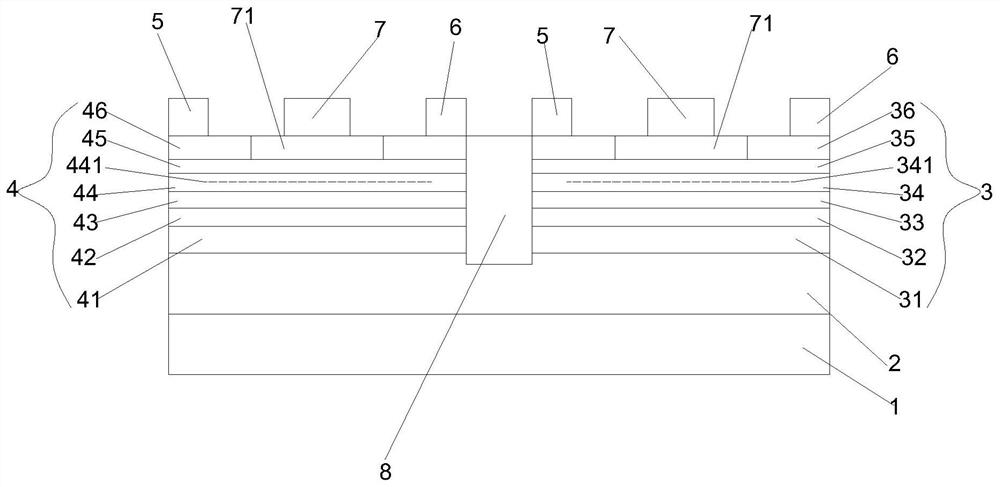
[0066] A kind of antimonide quantum well CMOS device structure, see figure 1 shown, including:

[0067] Using GaAs as the substrate 1;

[0068] A buffer layer 2 is provided on the substrate 1, and the thickness of the buffer layer is 1.0 μm;

[0069] The buffer layer 2 is relatively independently provided with a p-channel antimonide quantum well layer 3 and an n-channel antimonide quantum well layer 4;

[0070] The p-channel antimonide quantum well layer 3 includes:

[0071] Laminated on the buffer layer 2 sequentially from bottom to top

[0072] The first lower barrier layer 31 is made of AlGaSb material with a thickness of 50nm,

[0073] The first channel layer 32 is made of InGaSb material with a thickness of 10nm.

[0074] The first isolation layer 33 is made of AlGaSb material with a thickness of 2nm.

[0075] The first upper barrier layer 34 is made of AlGaSb material with a thickness of 5nm,

[0076] The first interface control layer 35 is made of InAs material w...

Embodiment 2

[0124] A kind of antimonide quantum well CMOS device structure, same as embodiment 1, difference is:

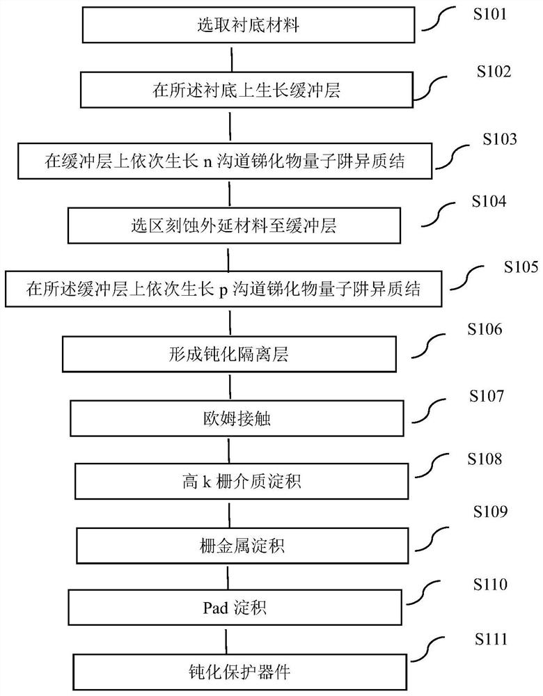
[0125] The preparation method of above-mentioned antimonide quantum well CMOS device structure, see image 3 shown, including the following steps:

[0126] S201 Select GaAs substrate

[0127] S202 using molecular beam epitaxy to grow a buffer layer of 1 μm AlGaSb on the GaAs substrate.

[0128]S203 Using molecular beam epitaxy technology on the buffer layer, sequentially grow n-channel antimonide quantum well layers to form a heterojunction; grow a second lower barrier layer AlInSb on the surface of the buffer layer; grow the second lower barrier layer on the second lower barrier layer growing a second channel layer InAsSb on the top; growing a second isolation layer AlInSb on the second channel layer; growing a second upper barrier layer AlInSb on the second isolation layer; growing a second upper barrier layer AlInSb on the second upper barrier Doping Si in the layer to ...

Embodiment 3

[0153] Same as Example 1, the difference is that

[0154] The p-channel antimonide quantum well layer on the buffer layer, the n-channel antimonide quantum well layer and the passivation isolation layer between the p-channel antimonide quantum well layer and the n-channel antimonide quantum well layer are according to the following steps be made of,

[0155] After the preparation of the p-channel antimonide quantum well layer is completed, the epitaxial material of the p-channel antimonide quantum well layer is selectively etched to the buffer layer to form a trench area where the n-channel antimonide quantum well layer can grow, and the p-channel is formed by PECVD. The etched side of the antimonide quantum well layer is passivated, and the passivation layer SiO is deposited 2 , forming a passivation isolation layer, and then growing an n-channel antimonide quantum well layer on the buffer layer to realize a passivation isolation region between the n-channel antimonide quant...


PUM

PropertyMeasurementUnit
thicknessaaaaaaaaaa
thicknessaaaaaaaaaa
thicknessaaaaaaaaaa

Abstract

The invention discloses a structure of an antimonide quantum well CMOS device and a preparation method thereof, and belongs to the technical field of microelectronics. The device structure comprises a substrate; a buffer layer arranged on the substrate; a p-channel antimonide quantum well layer and an n-channel antimonide quantum well layer which are relatively independently arranged on the buffer layer; wherein a passivation isolation layer is arranged between the p-channel antimonide quantum well layer and the n-channel antimonide quantum well layer. According to the antimonide quantum well structure provided by the invention, on one hand, the dislocation density caused by lattice mismatch can be reduced through component regulation and control, and on the other hand, the channel and the high-k gate dielectric are effectively isolated through the barrier layer, and a two-dimensional electron/hole gas is formed on the surface of the channel, so that the mobility is improved, and the performance of a device is improved. The invention further provides the preparation method of the antimonide quantum well CMOS device, and epitaxial growth of n channel and p channel materials of the same system is achieved.

Description

technical field [0001] The invention belongs to the technical field of microelectronics, relates to a semiconductor device, in particular to a structure of an antimonide quantum well CMOS device and a preparation method thereof. Background technique [0002] The feature size of traditional Si channel MOSFET devices continues to shrink following Moore's Law, and its comprehensive performance such as speed and power consumption is approaching the physical limit. The complementary metal-oxide-semiconductor (CMOS) device composed of n-MOSFET and p-MOSFET is a basic unit of integrated circuits. Therefore, in order to maintain the continuous development of microelectronics technology, researchers are considering nanoscale new structure Si channel At the same time, using non-Si materials with higher mobility as n-channel and p-channel has become an important research direction to improve the performance of CMOS devices. [0003] The electron mobility of III-V compounds is more tha...

Claims


Application Information

Patent Timeline
Patent Type & Authority Applications(China)
IPC IPC(8): H01L29/10H01L29/06H01L29/201H01L27/092H01L21/8252
CPCH01L21/8252H01L27/0928H01L29/0642H01L29/0665H01L29/0684H01L29/1033H01L29/201
Inventor 张静
Owner SHAANXI UNIV OF SCI & TECH
Why Eureka
Try Eureka