

Heat transfer experimental device for electronic packaging microscale solder joint
An experimental device and electronic packaging technology, applied in the direction of material thermal conductivity, etc., can solve the problems of high temperature gradient and affect the reliability of small solder joints, and achieve the effect of improving accuracy, facilitating heat transfer, and ensuring cooling effect.
- Summary
- Abstract
- Description
- Claims
- Application Information
AI Technical Summary
Problems solved by technology
Method used
Image

Examples
Embodiment 1
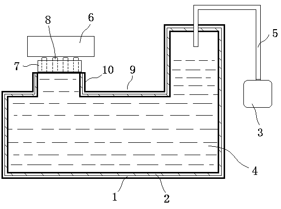
[0021] Embodiment one, see figure 1 , the thermomigration experimental device of micro-solder joints in electronic packaging shown, the device includes a heating mechanism 6, a fixture 7 and a cooling mechanism from top to bottom, and the fixture 7 is arranged in the space between the heating mechanism 6 and the cooling mechanism , used to fix the sample 8.
[0022] The cooling mechanism includes an outer shell 1, an inner shell 2 and a refrigerator 3. The inner shell 2 is provided with a cavity for containing the cooling liquid 4, and the outer shell 1 is sheathed on the outside. The outer shell 1 and the inner shell Body 2 fits snugly with no gap between the two. The refrigerating machine 3 passes through the outer shell 1 and the inner shell 2 to communicate with the cavity through the connecting pipeline 5 , and the temperature of the cooling liquid 4 is adjusted through the refrigerating machine 3 to realize the adjustable temperature of the cold end. The outer casing 1...
Embodiment 2
[0028] Embodiment two, adopt the thermomigration experimental device of electronic package micro-soldering point described in embodiment one to carry out the thermomigration experiment of micro-soldering point, it comprises the following steps:
[0029] S1, adjust the heating temperature of the heating core of the heating mechanism to 230°C, and wait for the heating mechanism to stabilize to the set temperature for standby;
[0030] S2, ethylene glycol and deionized water are used in a volume ratio of 2:1 to prepare cooling liquid. The freezing point of the cooling liquid is -68°C. Fill the cooling liquid into the cavity of the inner shell, turn on the refrigerator, and set the temperature to - 60°C, standby when the temperature drops to -60°C;
[0031] S3, using a Cu / Sn / Cu sandwich structure sample with a height of 5mm, wherein the height of the micro-soldering point is 50 μm, and the position of the micro-soldering point is located in the center of the sample, and the sample...
Embodiment 3
[0034] Embodiment three, using the thermomigration experimental device of electronic package micro-soldering point described in embodiment one to carry out the thermal migration experiment of micro-soldering point, it comprises the following steps:
[0035] S1, adjust the heating temperature of the heating core of the heating mechanism to 230°C, and wait for the heating mechanism to stabilize to the set temperature for standby;
[0036] S2, ethylene glycol and deionized water are configured as cooling liquid according to the volume ratio of 19:1. The freezing point of the cooling liquid is -99.5°C. Fill the cooling liquid into the cavity of the inner shell, turn on the refrigerator, and set the temperature to - 80°C, standby when the temperature drops to -80°C;
[0037] S3, using a Cu / Sn / Cu sandwich structure sample with a height of 4mm, wherein the height of the micro-soldering point is 15 μm, and the position of the micro-soldering point is located in the center of the sampl...
PUM
| Property | Measurement | Unit |
|---|---|---|
| freezing point | aaaaa | aaaaa |
| height | aaaaa | aaaaa |
| freezing point | aaaaa | aaaaa |
Abstract
Description
Claims
Application Information