

Double-frequency duplexer based on substrate integrated waveguide
A substrate-integrated waveguide and duplexer technology, which is applied to waveguide-type devices, electrical components, circuits, etc., can solve the problems of bulky metal waveguides, difficult integration, and failure of microstrip lines, and achieves simple design structure and increased size Gain, easy industrial processing effect
- Summary
- Abstract
- Description
- Claims
- Application Information
AI Technical Summary
Problems solved by technology
Method used
Image

Examples
Embodiment 1
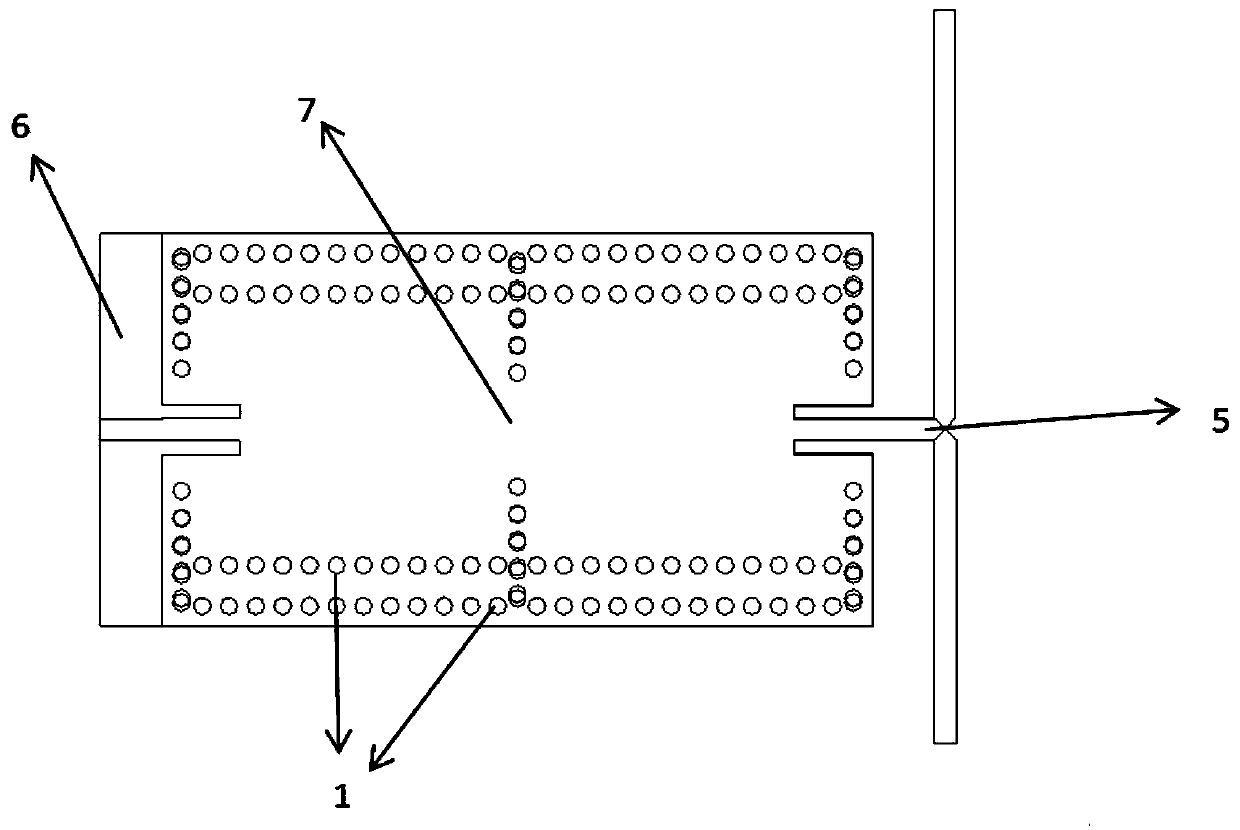
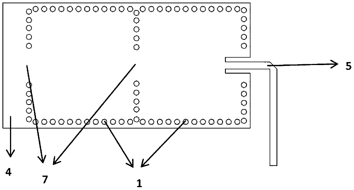
[0032] Such as Figure 4 As shown, a wave port is on the middle metal layer of the SIW cavity, that is, one microstrip line is on the middle metal layer of the two dielectric plates, and two equal slits are respectively set on both sides of the microstrip line, through which the microstrip The coplanar waveguide forms a wave port, and at the same time, metal through holes are arranged on two equal sides of the slit, and the same metal through holes are arranged on the other three sides, wherein the distances between the two through holes are equal. A T-shaped output port is set in the center of the upper and lower surfaces of the dual-frequency SIW duplexer to realize the power division of the signal. Such as Figure 6 As shown in the S-parameter simulation waveform diagram, the dual frequency points are 11.6GHz and 13.5GHz respectively, and the return loss is greater than 20dB and 22dB respectively, and its working performance is good.
Embodiment 2
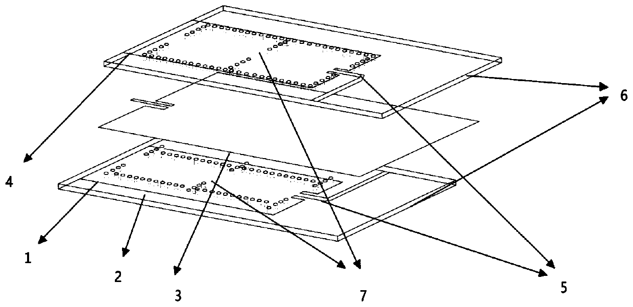
[0034] Such as image 3 and 5 As shown, the duplexer is composed of upper and lower layers of double cavities, the middle metal layer is used as the isolation layer of the upper and lower layers, each cavity is composed of metal through holes around the dielectric substrate and upper and lower metal layers, and the cavities of the same layer are connected by coupling The window realizes signal transmission. Such as Figure 6 It is the S-parameter simulation waveform diagram of a compact dual-frequency duplexer with a double-layer substrate integrated waveguide. The dual frequency points are 11.6GHz and 13.5GHz, the return loss is greater than 20dB and 22dB, and the insertion loss is less than -1dB. Good performance.
[0035] The invention aims to provide a dual-frequency duplexer based on substrate integrated waveguide, which solves the problem of low passband gain of SIW filter and aims to lay a foundation for future research on filters with higher passband gain.
PUM
| Property | Measurement | Unit |
|---|---|---|
| Impedance | aaaaa | aaaaa |
| Return loss | aaaaa | aaaaa |
Abstract
Description
Claims
Application Information