Probe card, test equipment comprising probe card, and test method

A technology for testing equipment and probe cards, applied in the field of probe cards, can solve problems such as low test accuracy, damage to semiconductor chips, ignition of semiconductor chips, etc., to avoid the phenomenon of ignition, ensure safety, and improve test accuracy.

Pending Publication Date: 2019-09-13
GLOBAL ENERGY INTERCONNECTION RES INST CO LTD
View PDF6 Cites 10 Cited by
  • Summary
  • Abstract
  • Description
  • Claims
  • Application Information

AI Technical Summary

Problems solved by technology

[0005] Since the current test equipment is mostly exposed to the air, during high-voltage testing, when the air is humid and there are impurities, the semiconductor chip is prone to sparking, resulting in damage to the semiconductor chip, and the test accuracy is low

Method used


Image

  • Probe card, test equipment comprising probe card, and test method
  • Probe card, test equipment comprising probe card, and test method
  • Probe card, test equipment comprising probe card, and test method

Examples


Embodiment 1

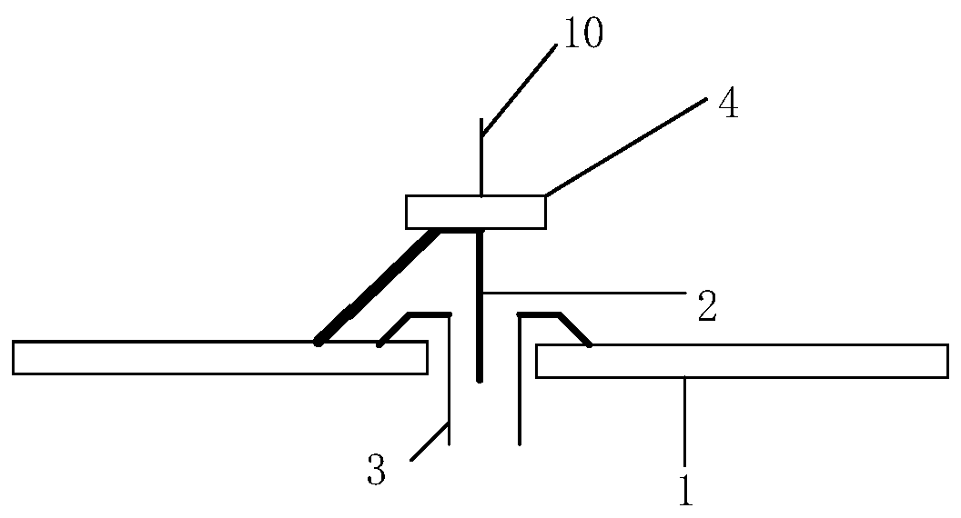
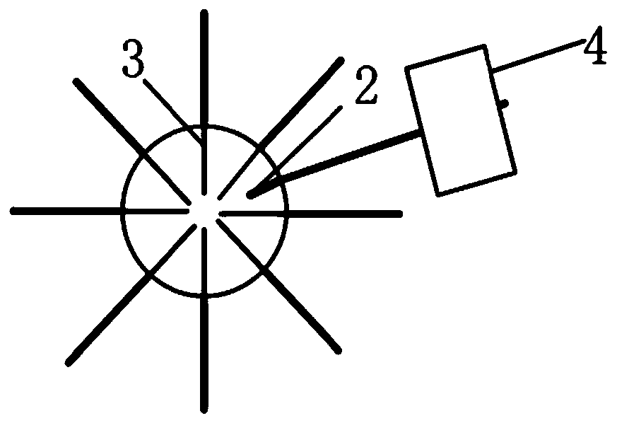
[0046] Embodiment 1 of the present invention provides a probe card, its cross-sectional view and top view are as follows figure 1 and figure 2 As shown, the probe card includes a PCB board 1, a hollow needle 2 and a probe 3; the hollow needle 2 and the probe 3 are respectively connected to the PCB board 1, and the hollow needle 2 and the probe 3 are adjacently arranged; the hollow needle 2 is used for For spraying the flame retardant gas, the flame retardant gas in Embodiment 1 of the present invention can be nitrogen.

[0047] The probe card provided by Embodiment 1 of the present invention also includes a pressure chamber 4 ; the needle tail of the hollow needle 2 is placed in the pressure chamber 4 .

[0048] The probe card provided by Embodiment 1 of the present invention also includes a first support arm and a second support arm; the hollow needle 2 is connected to the contact point provided on the PCB board 1 through the first support arm, and the probe 3 is connected ...

Embodiment 2

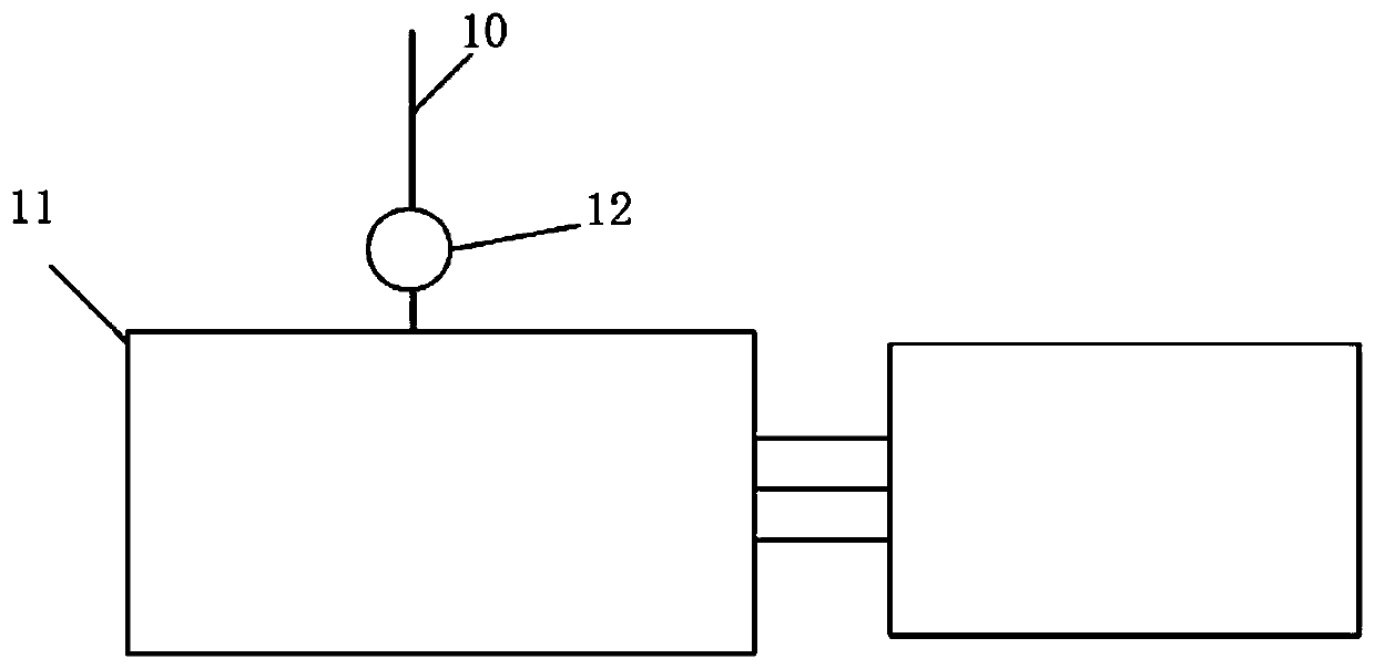
[0057] Embodiment 2 of the present invention provides a test device, including a probe card, a pipeline 10 and a high-pressure test device 11; the specific connection relationship is: the pressure chamber 4 of the probe card is connected to the nitrogen pipeline 10, and the probe card passes through the interface Insert the high-voltage testing device 11, and the pipeline 10 is filled with flame-retardant gas.

[0058] The pipeline 10 is provided with a pressure regulating valve 12 for adjusting the pressure of the flame retardant gas according to the conditions of the tested products.

[0059] The above-mentioned high-voltage test device 11 includes a high-voltage direct current source, a detection device and a slide table; the high-voltage direct current source is connected to the detection device to provide power for the detection device; the detection device is provided with a card slot, and the probe card is inserted into the card slot through the interface The slide table ...

Embodiment 3

[0061] Embodiment 3 of the present invention provides a method for testing a semiconductor chip to be tested by using the test device of Embodiment 2. The specific process is as follows:

[0062] S101: placing the probe card in the high voltage testing device 11;

[0063] S102: placing the semiconductor chip to be tested on the carrier stage of the high voltage testing device 11;

[0064] S103: Open the pressure regulating valve 12, and adjust the pressure of the flame retardant gas in the pipeline 10 to a preset pressure value (such as 0.01mpa) according to the demand of the semiconductor chip to be tested;

[0065] S104: Adjust the height of the slide table so that the probe 3 of the probe card is in contact with the semiconductor chip to be tested;

[0066] S105: Turn on the high voltage testing device 11 to test the static parameters of the semiconductor chip to be tested.

[0067] For the convenience of description, each part of the device described above is divided int...


PUM


Abstract

The invention provides a probe card, test equipment comprising the probe card, and a test method. The probe card comprises a PCB board, a hollow needle and a probe; the hollow needle and the probe arerespectively connected with the PCB board, and the hollow needle and the probe are adjacently arranged; the hollow needle is used for releasing flame-retardant gas. During testing, the needle tip ofthe hollow needle can be used to spray the flame-retardant gas to form a flame-retardant gas protective atmosphere, so that an ignition phenomenon of a semiconductor chip during the testing can be effectively reduced. The test equipment comprises the probe card, a pipeline and a high-voltage test device, wherein the pressure cavity of the probe card is connected with the pipeline, and the probe card is inserted into the high-voltage test device through an interface. The test equipment is used to prevent the ignition phenomenon during the testing of the semiconductor chip, and the safety of thesemiconductor chip is guaranteed, and the test precision is greatly improved.

Description

technical field [0001] The invention relates to the technical field of high-voltage semiconductors, in particular to a probe card, testing equipment including the probe card, and a testing method. Background technique [0002] In recent years, semiconductor manufacturing technology has advanced by leaps and bounds, and it is several years ahead of Moore's Law. At this stage, it has advanced to below 32nm. At present, the products are thin, light and small. The IC volume is getting smaller and stronger, and the number of pins is increasing. In order to reduce the area occupied by the chip package and improve the performance of the IC, flip-chip packaging is generally used in graphics at this stage. Chips, chipsets, memory and CPU, etc. The unit price of the above-mentioned high-end packaging method is high. If the chip test can be carried out before packaging, if there are defective products in the wafer, they will be marked immediately, and these marked defective products w...

Claims


Application Information

Patent Timeline
Patent Type & Authority Applications(China)
IPC IPC(8): G01R1/073
CPCG01R1/073
Inventor 李嘉琳李玲吴昊郑柳焦倩倩杨霏潘艳
Owner GLOBAL ENERGY INTERCONNECTION RES INST CO LTD
Why Eureka
Try Eureka