Temperable LOW-E glass and preparation method thereof
A glass and glass matrix technology, applied in the field of temperable LOW-E glass and its preparation, can solve the problems of large color changes and achieve the effect of ensuring consistency
- Summary
- Abstract
- Description
- Claims
- Application Information
AI Technical Summary
Problems solved by technology
Method used
Image

Examples
Embodiment 1
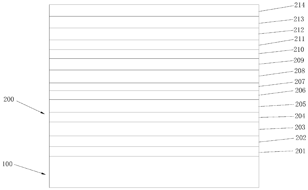
[0033] The structure of the composite film layer 200 on the surface of the glass substrate 100 in this example is: SiNx layer / TiOx layer / ZnOx layer / Ag layer / NiCr layer / AZO layer / SiNx layer / NiCr layer / SiNx layer / ZnOx layer / Ag layer / NiCr layer / AZO layer / SiNx layer.
[0034] The thickness of each film layer in the composite film layer 200 is 34.2nm / 9.8nm / 15.2nm / 9.2nm / 1.8nm / 8.9nm / 29.3nm / 1.1nm / 33.7nm / 15.0nm / 10.1nm / 1.3nm / 9.2nm nm / 27.4nm.
[0035] The preparation method of temperable LOW-E glass in this embodiment is as follows:
[0036] 1. The first dielectric layer 201 is plated on the glass substrate 100 by magnetron sputtering process: under the control of an intermediate frequency AC power supply, the silicon target is sputtered in a mixed atmosphere of argon and nitrogen (Ar:N2=9:7) Spray deposition, the first dielectric layer with a film thickness of 34.2nm is a SiNx layer;
[0037] 2. Coating the transition layer 202 on the first dielectric layer by magnetron sputtering: U...
Embodiment 2
[0060] The structure of the composite film layer 200 on the surface of the glass substrate 100 in this example is: SiNx layer / TiOx layer / ZnOx layer / Ag layer / NiCr layer / AZO layer / SiNx layer / NiCr layer / SiNx layer / ZnOx layer / Ag layer / NiCr layer / AZO layer / SiNxOy layer.
[0061] The thickness of each film layer in the composite film layer 200 is 29.7nm / 4.6nm / 14.8nm / 7.1nm / 1.8nm / 8.8nm / 30.8nm / 1.3nm / 34.3nm / 15.9nm / 9.8nm / 1.3nm / 9.3nm nm / 25.6nm.
[0062] The preparation method of temperable LOW-E glass in this embodiment is as follows:
[0063] 1. The first dielectric layer 201 is plated on the glass substrate 100 by magnetron sputtering process: under the control of an intermediate frequency AC power supply, the silicon target is sputtered in a mixed atmosphere of argon and nitrogen (Ar:N2=9:7) Spray deposition, depositing a first dielectric layer 201 (SiNx layer) with a film thickness of 29.7 nm;
[0064] 2. Using the magnetron sputtering process, the transition layer 202 is plated on...
PUM
| Property | Measurement | Unit |
|---|---|---|
| Thickness | aaaaa | aaaaa |
| Thickness | aaaaa | aaaaa |
| Thickness | aaaaa | aaaaa |
Abstract
Description
Claims
Application Information
 - R&D
- Intellectual Property
- Life Sciences
- Materials
- Tech Scout
- Unparalleled Data Quality
- Higher Quality Content
- 60% Fewer Hallucinations
Browse by: Latest US Patents, China's latest patents, Technical Efficacy Thesaurus, Application Domain, Technology Topic, Popular Technical Reports.
© 2025 PatSnap. All rights reserved.Legal|Privacy policy|Modern Slavery Act Transparency Statement|Sitemap|About US| Contact US: help@patsnap.com