A method of manufacturing an embedded flexible conductive circuit

A technology of flexible conduction and manufacturing methods, which is applied in printed circuit manufacturing, cleaning methods using liquids, printed circuits, etc., can solve the problems of poor flexibility of conductive lines, poor electrical conductivity, and complicated manufacturing processes, and achieve low cost and solve integrated problems. The effect of poor performance and easy effective integration

Active Publication Date: 2020-08-04
XI'AN POLYTECHNIC UNIVERSITY
View PDF6 Cites 0 Cited by
  • Summary
  • Abstract
  • Description
  • Claims
  • Application Information

AI Technical Summary

Problems solved by technology

[0004] The purpose of the present invention is to provide a method for manufacturing an embedded flexible conductive circuit, which solves the problems of poor flexibility, poor conductivity and complicated manufacturing process of the existing conductive circuit

Method used


Image

  • A method of manufacturing an embedded flexible conductive circuit
  • A method of manufacturing an embedded flexible conductive circuit

Examples


Embodiment 1

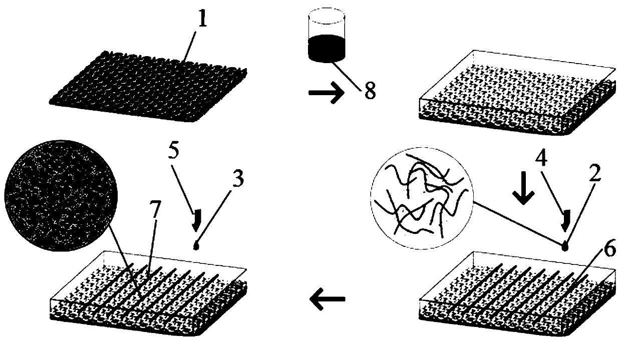
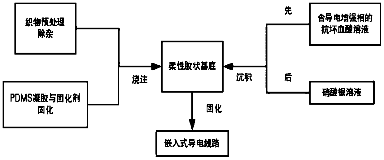
[0049] (1) Preparation of flexible substrate 1

[0050] Select a piece of paper, i.e. the flexible substrate 1, and cut it into a size of 70mm×70mm for later use;

[0051] Stir polydimethylsiloxane and Dow Corning 184 silicone rubber curing agent at a mass ratio of 9:1, and use a vacuum filter to remove air bubbles to obtain packaging material 8, which is placed on the upper surface of the flexible substrate 1 Pouring encapsulation material 8 to completely cover;

[0052] (2) Preparation of Ink A2

[0053] Dissolve ascorbic acid powder, polyvinylpyrrolidone, silver nanowires, carbon nanotubes and graphene in deionized water at a mass ratio of 280:70:5:2:1, and stir evenly to obtain a precursor solution; Ink A2 is obtained after supersonicating the precursor solution in an ultrasonic oscillator for 1 hour, and is ready for use; wherein, the mass volume concentration of ascorbic acid powder is 20% w / v, the mass volume concentration of nano-silver is 0.1% w / v, and the carbon na...

Embodiment 2

[0059] (1) Preparation of flexible substrate 1

[0060] Select the plain weave fabric in the textile material, that is, the flexible substrate 1, cut it into a size of 70mm×70mm, soak it in alcohol with a volume fraction of 75%, and test it in an ultrasonic oscillator with a frequency of 40KHz and a power of 70W. Sonicate for 15 minutes, wash it with deionized water, let it stand at room temperature for 0.8 hours, and set aside;

[0061] Stir polydimethylsiloxane and Dow Corning 184 silicone rubber curing agent evenly at a mass ratio of 10:1, and use a vacuum filter to remove air bubbles to obtain packaging material 8, which is placed on the upper surface of the flexible substrate 1 Pouring encapsulation material 8 to completely cover;

[0062] (2) Preparation of Ink A2

[0063] Dissolve ascorbic acid powder, polyvinylpyrrolidone, silver nanowires, carbon nanotubes and graphene in deionized water at a mass ratio of 300:80:10:3:1, and stir evenly to obtain a precursor solutio...

Embodiment 3

[0069] (1) Preparation of flexible substrate 1

[0070] Select polyimide, i.e. the flexible substrate 1, and cut it into a size of 70mm×70mm for later use;

[0071] Stir polydimethylsiloxane and Dow Corning 184 silicone rubber curing agent evenly at a mass ratio of 15:1, and use a vacuum filter to remove air bubbles to obtain packaging material 8, which is placed on the upper surface of the flexible substrate 1 Pouring encapsulation material 8 to completely cover;

[0072] (2) Preparation of Ink A2

[0073] Dissolve ascorbic acid powder, polyvinylpyrrolidone, silver nanowires, carbon nanotubes and graphene in deionized water at a mass ratio of 350:90:15:8:1, and stir evenly to obtain a precursor solution; Ink A2 is obtained after supersonicating the precursor solution in an ultrasonic oscillator for 2 hours, and is ready for use; wherein, the mass volume concentration of ascorbic acid powder is 30% w / v, the mass volume concentration of nano-silver is 1% w / v, and the carbon n...


PUM


Abstract

The invention discloses a manufacturing method of an embedded flexible conductive circuit. The manufacturing method comprises the following steps: firstly, selecting an appropriate flexible substrate, processing and standing for later use; pouring a packaging material on the upper surface of the flexible substrate until the packaging material completely covers the flexible substrate; dissolving ascorbic acid powder, polyvinylpyrrolidone, silver nanowires, carbon nanotubes and graphene in deionized water, uniformly stirring to obtain a precursor solution, and carrying out ultrasonic treatment to obtain ink A; dissolving silver nitrate powder in deionized water, and uniformly stirring to obtain ink B; respectively putting the ink A and the ink B into a piezoelectric sprayer A and a piezoelectric sprayer B in a droplet jetting device; printing the ink A on the packaging material drop by drop, and then printing the ink B drop by drop according to the path of the ink A; and finally, putting the printed material into a curing oven for curing treatment, and cooling to obtain the embedded flexible conductive circuit. The problems that an existing conductive circuit is poor in flexibility and conductivity and complex in manufacturing process are solved.

Description

technical field [0001] The invention belongs to the technical field of flexible wearable electronic devices, and relates to a method for manufacturing an embedded flexible conductive circuit. Background technique [0002] Inkjet printing technology has the advantages of high flexibility, low cost, and environmental protection. It has received extensive attention in the fields of solar cells, organic light-emitting diodes, organic transistors and other electronic devices. The key to the realization of the functions of flexible electronic devices lies in the flexible preparation of conductive circuits. The selection of conductive ink suitable for jet printing is the research focus of this technology. [0003] At present, common conductive inks include: metal nanoparticle dispersion solution, organometallic compound solution and metal salt solution. However, the manufacturing cost of metal nanoparticle ink is high; organometallic compound ink needs to be decomposed at a higher...

Claims


Application Information

Patent Timeline
Patent Type & Authority Patents(China)
IPC IPC(8): H05K3/00H05K3/12B08B3/08B08B3/12H05K1/03H05K1/09
CPCB08B3/08B08B3/12H05K1/0313H05K1/038H05K1/0386H05K1/092H05K3/0011H05K3/125H05K3/1283
Inventor 肖渊李红英张威
Owner XI'AN POLYTECHNIC UNIVERSITY
Why Eureka
Try Eureka