Welding system and method of device pins

A technology of welding system and welding method, which is applied in the field of optical communication, can solve problems such as low production efficiency, poor welding quality, and damaged devices, and achieve the effects of improving production efficiency, ensuring welding quality, and occupying a small space

Pending Publication Date: 2019-09-27
O NET COMM (SHENZHEN) LTD
View PDF0 Cites 4 Cited by
  • Summary
  • Abstract
  • Description
  • Claims
  • Application Information

AI Technical Summary

Problems solved by technology

[0006] The technical problem to be solved by the present invention is to provide a device pin welding system and its method in view of the above-mentioned defects of the prior art, so as to overcome th

Method used


Image

  • Welding system and method of device pins
  • Welding system and method of device pins
  • Welding system and method of device pins

Examples


Embodiment Construction

[0034] Now in conjunction with the accompanying drawings, the preferred embodiments of the present invention will be described in detail.

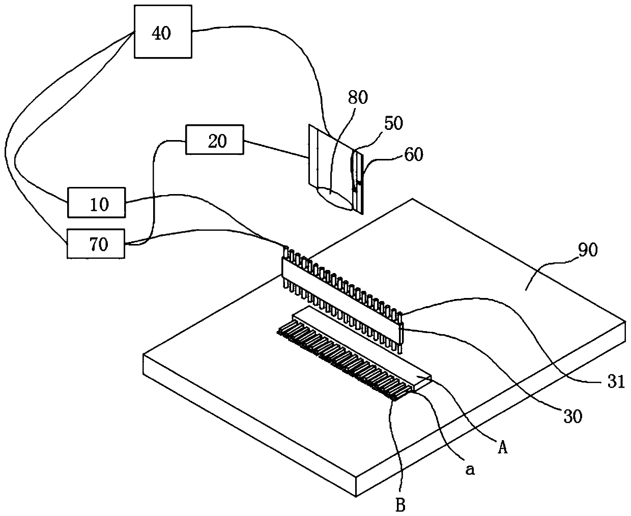
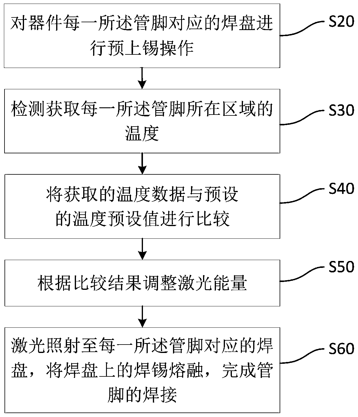
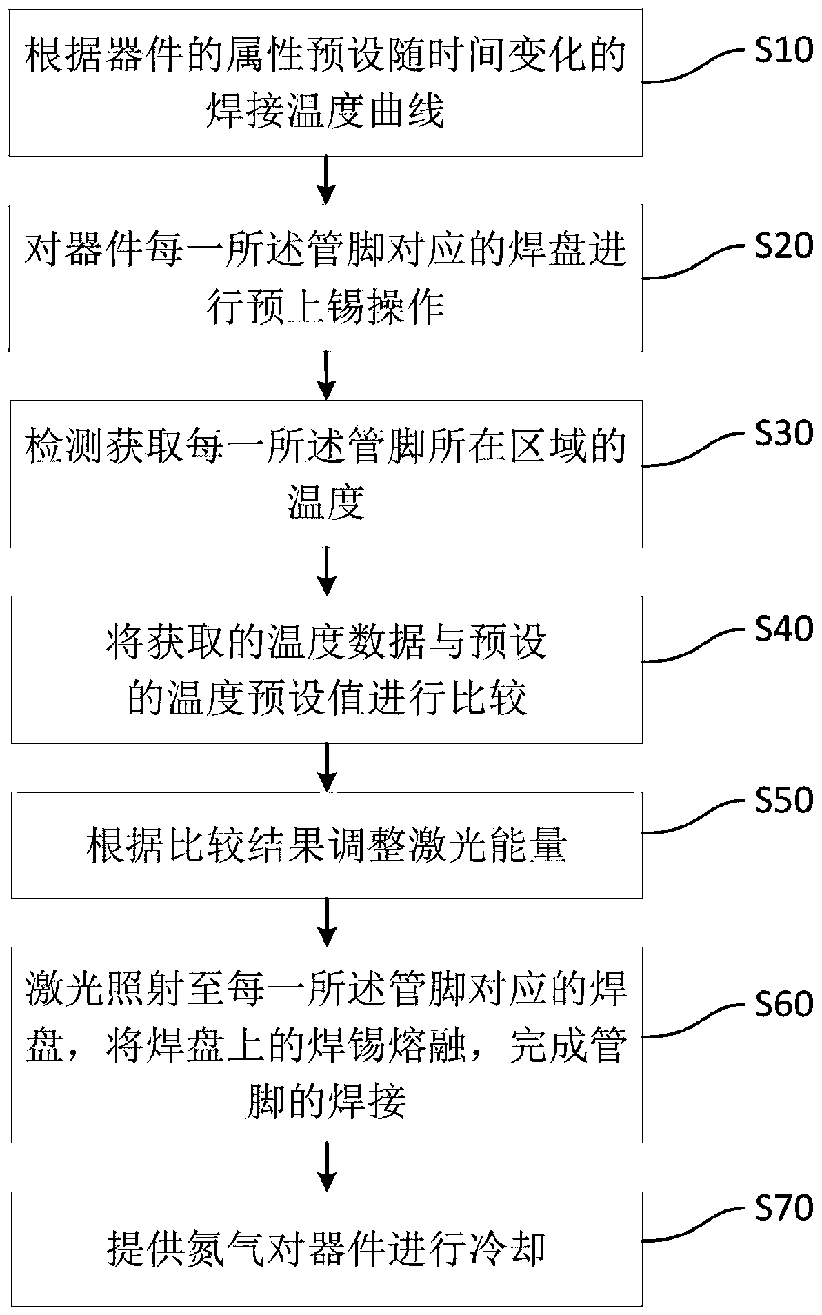
[0035] Such as figure 1 As shown, the present invention provides a preferred embodiment of a device pin soldering system.

[0036] Device A includes a plurality of pins a arranged in a row. The welding system includes:

[0037] Laser emitting device 10, used to generate laser light;

[0038] A temperature detection module 20, configured to detect the temperature of the area where each pin is located;

[0039] A lens module 30, the lens module 30 is provided with a plurality of lens structures 31 respectively corresponding to a pin a;

[0040] The main control module 40 is connected to the laser emitting device 10 and the temperature detection module 20 respectively, and is provided with a temperature preset value of the area where the pin is located;

[0041] Wherein, the main control module 40 obtains the temperature data detected by...


PUM


Abstract

The invention relates to the field of optical communication, in particular to a welding system and a method of device pins. The welding system comprises a laser emission device for generating laser light, a temperature detection module for detecting a temperature of an area where each pin is located, a lens module provided with a plurality of lens structures corresponding to the pins respectively, and a master control module connected with the laser emission device and the temperature detection module, wherein temperature preset values of the areas where the pins are located are set in the master control module; the master control module acquires temperature data detected by the temperature detection module, compares the temperature data with the temperature preset values, and controls and adjusts laser energy of the laser emission device according to comparison results; and the laser light is irradiated to welding discs corresponding to the pins for welding through the lens module. Precise contraposition of a device with a small pin distance, quick welding and controllable temperature can be achieved; the welding quality of the device is ensured; an occupied space is small; mass production is available; and the production efficiency is improved.

Description

technical field [0001] The invention relates to the field of optical communication, in particular to a device pin welding system and method thereof. Background technique [0002] At present, the butterfly devices in the optoelectronics industry have row-shaped leads / pins, and these row-shaped leads / pins need to be soldered to the corresponding metal pads on the surface of the PCB board to form a stable and firm electrical connection. [0003] With the rapid increase of communication rate, the signal bandwidth that needs to be carried and transmitted in the same physical space is getting larger and larger. The miniaturization and low power consumption of optical devices have become an inevitable trend in the industry, and the requirements are becoming more and more stringent. At the same time, it is constantly challenging the traditional welding process. After the miniaturization of the device, the pins are getting thinner and the spacing is getting smaller and smaller, and ...

Claims


Application Information

Patent Timeline
IPC IPC(8): B23K1/005B23K3/08B23K101/36
CPCB23K1/0056B23K3/08B23K2101/36
Inventor 郁勤荣朱月林王衍勇孙贺
Owner O NET COMM (SHENZHEN) LTD
Why Eureka
Try Eureka