Substrate and peeling method
A technology of substrates and flexible substrates, applied in photovoltaic power generation, electrical components, climate sustainability, etc., can solve problems such as limiting the effective improvement of stripping efficiency, high price of laser stripping equipment, and inability to effectively improve problems, so as to reduce the difficulty of stripping, The effect of improving the stripping efficiency and reducing the preparation cost
- Summary
- Abstract
- Description
- Claims
- Application Information
AI Technical Summary
Problems solved by technology
Method used
Image

Examples
preparation example Construction
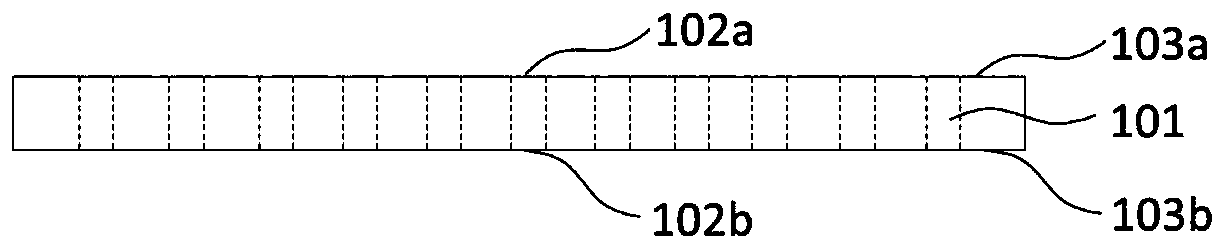
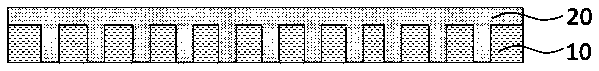
[0032] When using the substrate 10 to prepare flexible devices, the surface energy of the first surface 103a is reduced or the surface energy of the inner surface of the channel 101 is increased by means of surface treatment, that is, the surface energy of the first surface 103a is smaller than that of the inner surface of the channel 101. Surface energy, thereby reducing the affinity of the film layer (such as: sacrificial layer 20) and the first surface 103a, or increasing the affinity of the film layer (sacrifice layer 20) in the channel 101 and the inner surface of the channel 101, in the subsequent stripping of the electroluminescent device During the process, when the force between the film layer (sacrifice layer 20 ) and the inner surface of the hole 101 is broken, the film layer (sacrifice layer 20 ) can be quickly separated from the substrate 10 , thereby improving the stripping efficiency.
[0033] In the present invention, there is no special limitation on the above-...
Embodiment 1
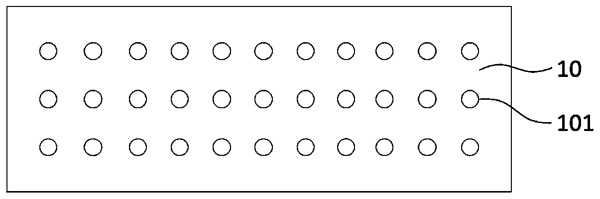
[0060] (1) Substrate specification selection: the size is 200*200*0.7mm, the surface energy of the first surface is 28mN / m, the first opening and the second opening are circular, the radius of the circle is 250μm, the first opening and the second opening The two openings are distributed axially symmetrically on the first surface and the second surface respectively, and the distribution density is 100 per square centimeter, and the line connecting the geometric centers of the first opening and the second opening pattern is perpendicular to the first surface.
[0061] (2) sacrificial layer is made: with the zinc oxide (ZnO) nanocrystal solution of coating 15wt% on above-mentioned substrate with slit coating equipment, the size of ZnO nanocrystal is 8nm, and solvent is amyl alcohol, and solution surface tension is 35mN / m, the thickness measured on the first surface after drying is 300 nm.
[0062] (3) Fabrication of the flexible substrate layer: a polyimide (PI) solution was coa...
Embodiment 2
[0066] (1) Substrate specification selection: the size is 200*200*0.7mm, the surface energy of the first surface is 28mN / m, the first opening and the second opening are circular, the radius of the circle is 100μm, the first opening and the second opening The two openings are distributed axially symmetrically on the first surface and the second surface respectively, and the distribution density is 500 per square centimeter, and the line connecting the geometric centers of the first opening and the second opening pattern is perpendicular to the first surface.
[0067] (2) The preparation method of the sacrificial layer is the same as the step (2) of embodiment 1.
[0068] (3) The manufacturing method of the flexible substrate layer is the same as the step (3) of Embodiment 1.
[0069] (4) The device manufacturing method is the same as step (4) of embodiment 1.
[0070] (5) The device stripping method is the same as step (5) of embodiment 1.
PUM
| Property | Measurement | Unit |
|---|---|---|
| Surface energy | aaaaa | aaaaa |
| Thickness | aaaaa | aaaaa |
| Size | aaaaa | aaaaa |
Abstract
Description
Claims
Application Information
 - R&D
- Intellectual Property
- Life Sciences
- Materials
- Tech Scout
- Unparalleled Data Quality
- Higher Quality Content
- 60% Fewer Hallucinations
Browse by: Latest US Patents, China's latest patents, Technical Efficacy Thesaurus, Application Domain, Technology Topic, Popular Technical Reports.
© 2025 PatSnap. All rights reserved.Legal|Privacy policy|Modern Slavery Act Transparency Statement|Sitemap|About US| Contact US: help@patsnap.com