Photovoltaic cell surface passivation system and passivation method

A photovoltaic cell, silicon nitride film technology, applied in photovoltaic power generation, circuits, electrical components and other directions, can solve the problems of high risk of unfinished products, low production efficiency, high production cost, reduce multiple processing, improve production efficiency, The effect of reducing adverse effects

Pending Publication Date: 2019-10-15
无锡松煜科技有限公司
View PDF0 Cites 6 Cited by
  • Summary
  • Abstract
  • Description
  • Claims
  • Application Information

AI Technical Summary

Problems solved by technology

[0006] In view of the shortcomings of the existing TOPCon battery surface passivation technology, such as cumbersome procedures, time-consuming and laborious, high production costs, low production efficiency, and high risk of unfinished products, the applicant provides a photovoltaic battery surface passivation system with reasonable structure and passivation technology. For the back of the silicon wafer, the multifunctional PECVD + annealing furnace heating and cooling process that deposits multiple films in the same chamber can be used to replace the existing LPCVD + cleaning and etch

Method used


Image

  • Photovoltaic cell surface passivation system and passivation method
  • Photovoltaic cell surface passivation system and passivation method
  • Photovoltaic cell surface passivation system and passivation method

Examples


Embodiment Construction

[0037] The specific implementation manner of the present invention will be described below in conjunction with the accompanying drawings.

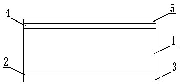
[0038] In this patent, the "multifunctional PECVD" refers to PECVD equipment that can deposit tunneling oxide layers, amorphous silicon layers, silicon nitride layers, etc. in the same chamber, and is used in this patent for the Silicon wafer 1 backside deposition for TOPCon cells. The "PEALD" refers to a PEALD device that can deposit all or any of the films of aluminum oxide, silicon oxide, silicon oxynitride and silicon nitride in the same chamber. In this patent, the PEALD device is used for the TOPCon battery The silicon wafer 1 is deposited on the front side.

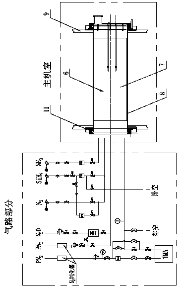
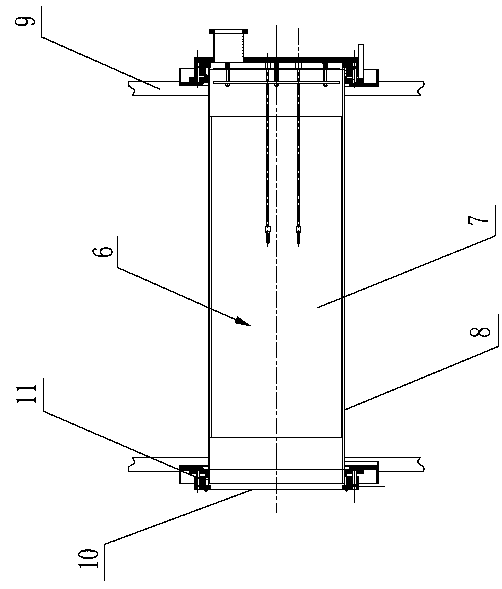
[0039] refer to figure 1 As shown, the photovoltaic cell surface passivation system of the present invention at least includes multifunctional PECVD equipment, annealing furnace and PEALD equipment, and the annealing furnace is located after the multifunctional PECVD process ...


PUM


Abstract

The invention discloses a photovoltaic cell surface passivation system and a passivation method. The photovoltaic cell surface passivation system at least comprises a multifunctional PECVD device, anannealing furnace and a PEALD device, wherein the annealing furnace is located after the multifunctional PECVD process; the process chambers of the annealing furnace and the multifunctional PECVD device are matched with the same corresponding graphite boat; the graphite boat carries a silicon wafer which is integrally transferred between the annealing furnace and the multifunctional PECVD device;the multifunctional PECVD device plates the back surface of the silicon wafer with a silicon oxide film and an amorphous silicon layer and performs in-situ doping on the amorphous silicon layer, the corresponding reaction temperature is 400 to 600 DEG C, the annealing furnace heats the plated silicon wafer to more than 600 DEG C, the amorphous silicon layer is converted to a polysilicon layer andthe temperature falls to 400 to 600 DEG C; and the PECVD device plates the front surface of the silicon wafer with an aluminum oxide film and a silicon nitride film. The overall structure of the device and the existing process steps are simplified, cleaning and etching processes are saved, adverse effect on front surface plating of the silicon wafer are reduced, the operation is more convenient, and the production efficiency is improved.

Description

technical field [0001] The invention relates to the technical field of solar cell passivation, in particular to a photovoltaic cell surface passivation system and a passivation method involving an ultra-thin tunnelable oxide layer and a highly doped polysilicon thin layer. Background technique [0002] Solar photovoltaic cell is a new type of battery that directly converts the sun's light energy into electrical energy. Silicon photovoltaic cells based on silicon are commonly used at present, including monocrystalline silicon, polycrystalline silicon and amorphous silicon photovoltaic cells. At present, relatively mature passivation film materials for photovoltaic cells include aluminum oxide (Al 2 o 3 ), silicon oxide (SiO 2 ), silicon oxynitride (SiO x N y ), silicon nitride (Si x N y )Wait. TOPCon (Tunnel Oxide Passivated Contact), as a new passivation technology, is mostly used in N-type crystalline silicon solar cells, which is characterized by plating silicon ox...

Claims


Application Information

Patent Timeline
IPC IPC(8): H01L31/0216H01L31/18H01L21/02
CPCH01L21/0217H01L21/02178H01L21/02356H01L31/02167H01L31/1876Y02E10/50Y02P70/50
Inventor 吴晓松陈庆敏李丙科李建新
Owner 无锡松煜科技有限公司
Why Eureka
Try Eureka