

Current sampling and limiting circuit of four-switch Buck-Boost converter
A current sampling and limiting circuit technology, which is applied in the field of current sampling and limiting circuits and analog integrated circuits, can solve the problems of increased power consumption and achieve the effects of short delay time, high sampling accuracy and short delay
- Summary
- Abstract
- Description
- Claims
- Application Information
AI Technical Summary
Problems solved by technology
Method used
Image

Examples
Embodiment 1
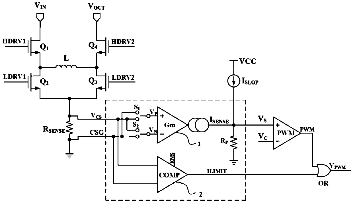
[0038] This embodiment provides a current sampling and limiting circuit of a four-switch Buck-Boost converter, such as figure 1 , 3 , Shown in 4, comprise transconductance amplifier Gm circuit 1, current limiting comparator COMP circuit 2; Wherein:
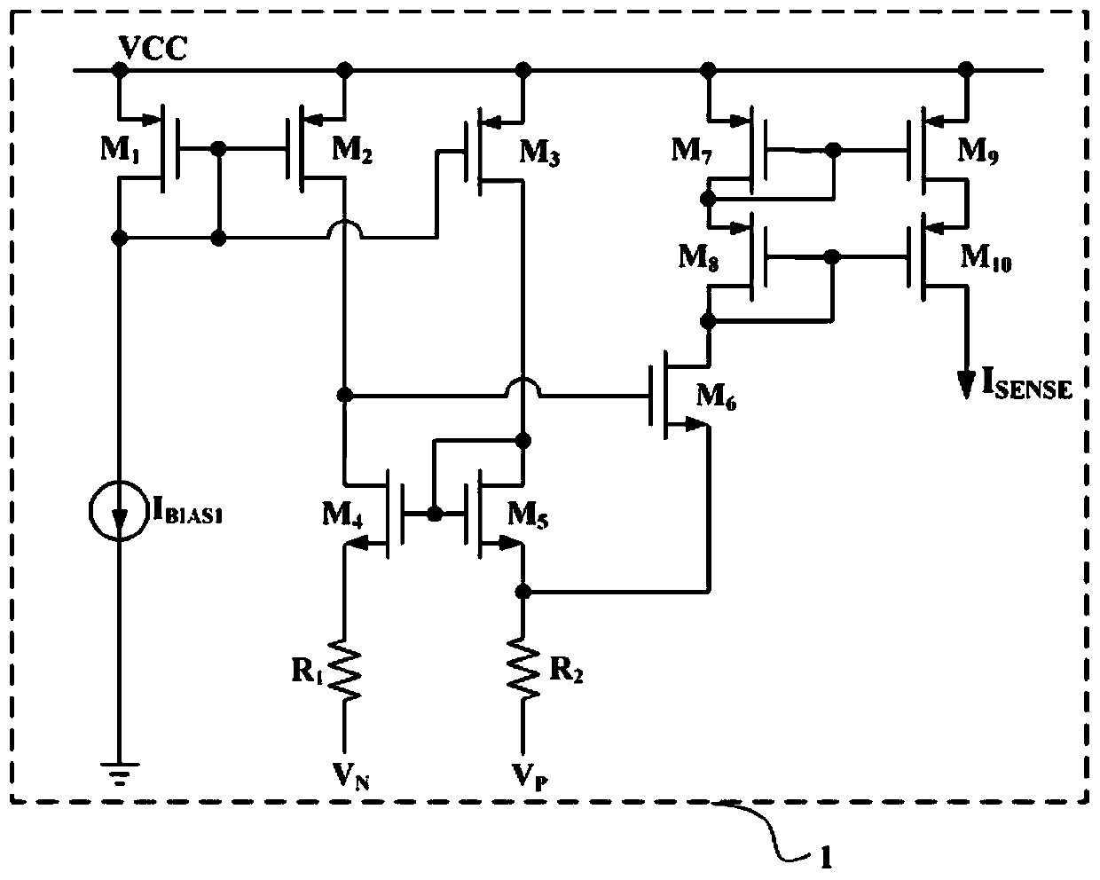
[0039] The transconductance amplifier Gm circuit is used to sample the sampling resistor R SENSE voltage on and converts to a sampled current I SENSE ;Sampling current I SENSE with slope compensation current I SLOP Through resistance R P Perform superposition and summation to obtain the voltage V S Input to the non-inverting input of the pulse width modulator PWM; the output voltage of the error amplifier V C Input for the inverting terminal of the pulse width modulator PWM, the voltage V S with V C The pulse control signal PWM is output by comparison with the pulse width modulator PWM;
[0040] The current limit comparator COMP circuit is used to limit the inductor current, the sense resistor R SENSE The voltage on the...
Embodiment 2
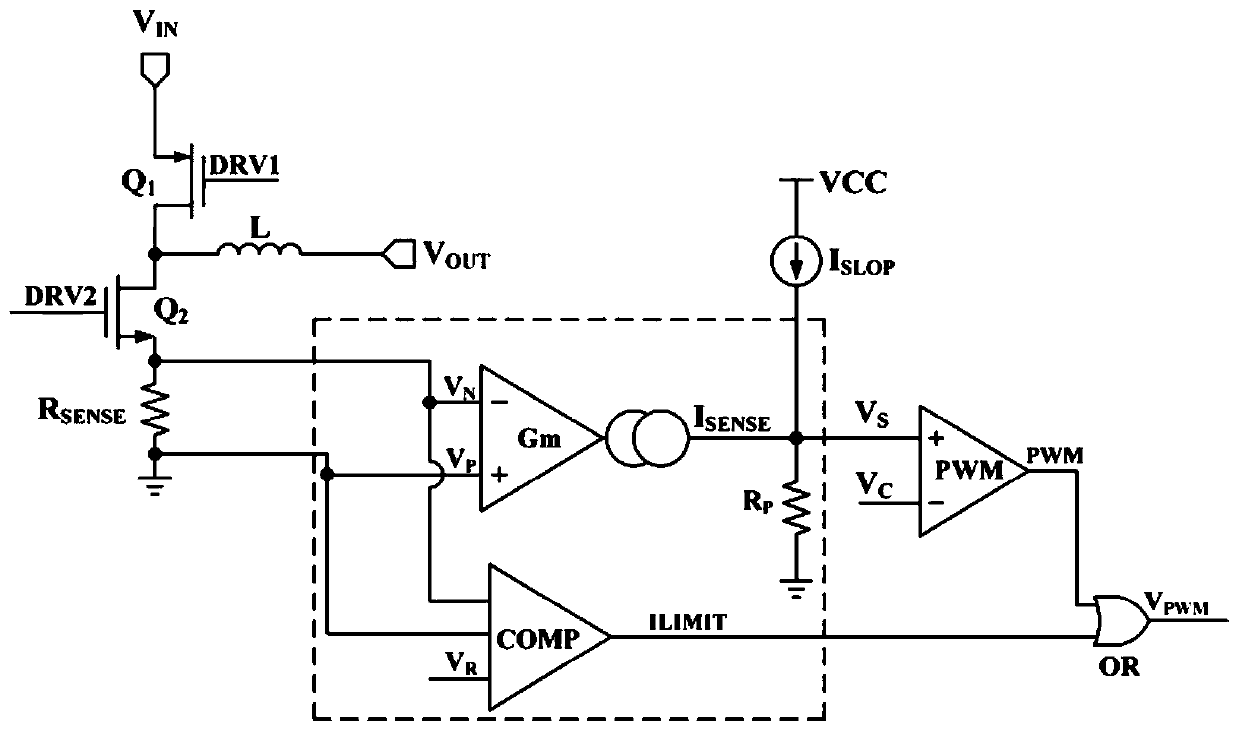
[0056] This embodiment provides a current sampling and limiting circuit of a four-switch Buck-Boost converter, such as figure 1 , 3 , Shown in 5, comprise transconductance amplifier Gm circuit 1, current limiting comparator COMP circuit 2;
[0057] The specific structure and connection method of the transconductance amplifier Gm circuit 1 of this embodiment are the same as those of the first embodiment.
[0058] As a specific solution of this embodiment, such as Figure 5 As shown, the current limiting comparator COMP circuit 2 of the present embodiment is comparator COMP1, comparator COMP2, inverter INV3, two-input AND gate AND1, two-input AND gate AND2 and two-input OR gate OR; wherein:
[0059] The non-inverting input terminal of the comparator COMP1 is connected with the reference voltage signal V TH_Buck phase connection, the inverting input is connected to the input signal V CS It is connected with the non-inverting input terminal of the comparator COMP2, and its ou...
PUM
 Abstract
Description
Claims
Application Information