
A cmos image sensor readout circuit compatible with two exposure modes

An image sensor and readout circuit technology, applied in image communication, television, electrical components, etc., can solve problems such as inability to achieve, and achieve the effects of low power consumption, low frame rate, and cost reduction

Active Publication Date: 2021-08-31
XIAN MICROELECTRONICS TECH INST
View PDF12 Cites 0 Cited by
  • Summary
  • Abstract
  • Description
  • Claims
  • Application Information

AI Technical Summary

Problems solved by technology

[0003] However, at present, these two exposure modes correspond to a set of readout circuit architecture design, which means that the same camera can only have one exposure mode. If another function needs to be implemented in special occasions, it cannot be realized.

Method used


Image

  • A cmos image sensor readout circuit compatible with two exposure modes
  • A cmos image sensor readout circuit compatible with two exposure modes
  • A cmos image sensor readout circuit compatible with two exposure modes

Examples


Embodiment Construction

[0028] In order to enable those skilled in the art to better understand the solutions of the present invention, the following will clearly and completely describe the technical solutions in the embodiments of the present invention in conjunction with the drawings in the embodiments of the present invention. Obviously, the described embodiments are only It is an embodiment of a part of the present invention, but not all embodiments. Based on the embodiments of the present invention, all other embodiments obtained by persons of ordinary skill in the art without making creative efforts shall fall within the protection scope of the present invention.

[0029] It should be noted that the terms "first" and "second" in the description and claims of the present invention and the above drawings are used to distinguish similar objects, but not necessarily used to describe a specific sequence or sequence. It is to be understood that the data so used are interchangeable under appropriate ...


PUM


Abstract

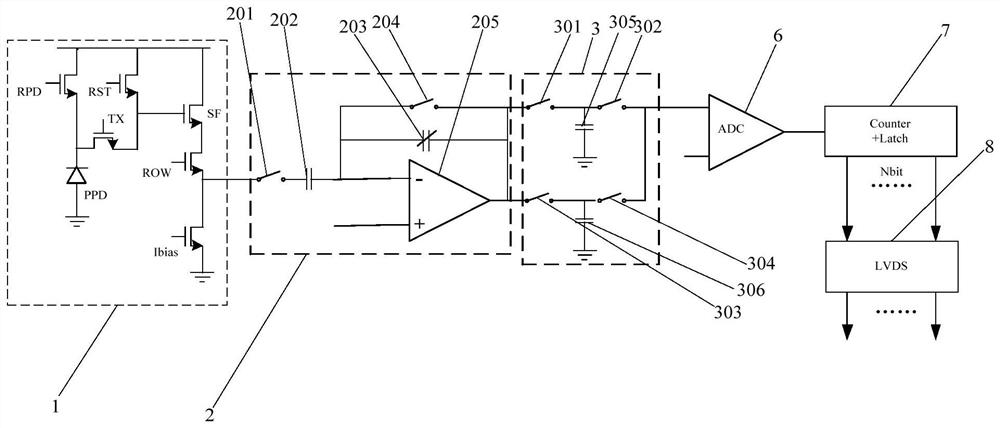
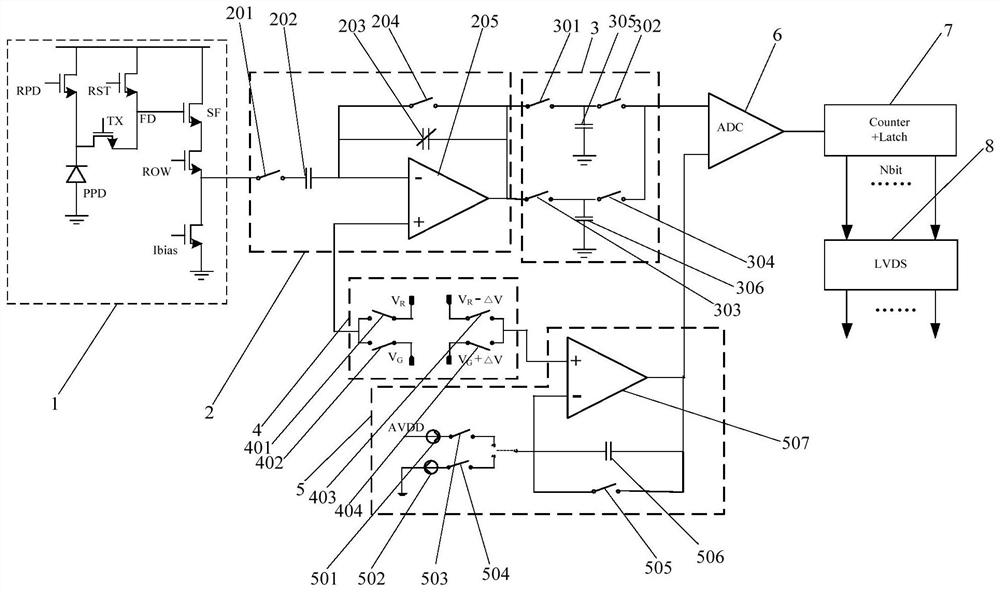
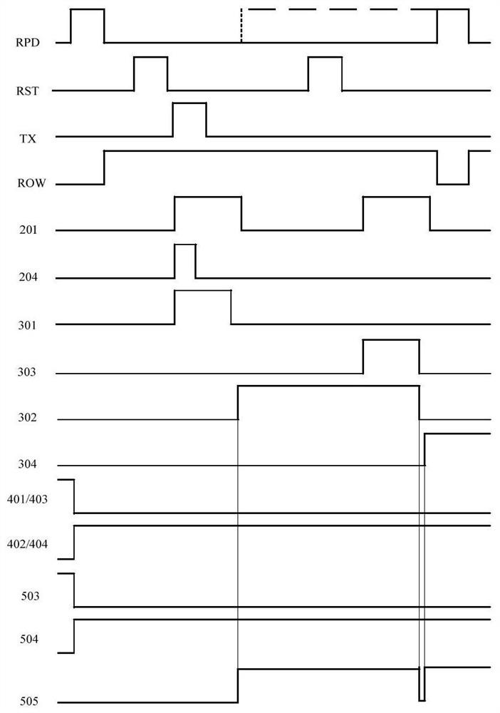
The invention discloses a CMOS image sensor readout circuit compatible with two exposure modes, comprising a pixel, a gain amplifier, a correlated double sampling circuit, a switching circuit, a slope generating circuit, an analog-to-digital converter and a counter; the output terminal of the pixel is connected to The first input end of the gain amplifier; the second input end of the gain amplifier is connected to the first output end of the switching circuit, the output end of the gain amplifier is connected to the input end of the correlated double sampling circuit, and the output end of the correlated double sampling circuit is connected to the analog-to-digital converter The first input end of the analog-to-digital converter is connected to the output end of the ramp generating circuit, the input end of the ramp generating circuit is connected to the second output end of the switching circuit; the output end of the analog-to-digital converter is connected to the input end of the counter . The readout circuit structure of the present invention can satisfy the output of two exposure modes, so that the two exposure modes can be integrated into the same camera; while being compatible with the two exposure modes, it basically does not occupy additional area and power consumption of the system.

Description

technical field [0001] The invention belongs to the field of CMOS image sensors and relates to a CMOS image sensor readout circuit compatible with two exposure modes. Background technique [0002] The image sensor is the core of the modern electronic imaging system, and the image sensor is mainly implemented based on two processes, CMOS process and charge-coupled device (CCD) process. CMOS image sensor technology has achieved rapid development in recent years due to its advantages of high integration, small size, and low power consumption. CMOS image sensors are currently divided into two exposure modes, one is the early rolling shutter exposure mode, and the output signal The noise ratio is high, but the frame rate is small. It is used for high-definition shooting of static objects or slow-moving objects, especially for geosynchronous satellite ground monitoring; the other is the global exposure mode, the output signal-to-noise ratio is relatively low, but High frame rate,...

Claims


Application Information

Patent Timeline
Patent Type & Authority Patents(China)
IPC IPC(8): H04N5/374H04N5/378
CPCH04N25/76H04N25/75
Inventor 何杰李婷李闯泽吴龙胜曹天骄
Owner XIAN MICROELECTRONICS TECH INST
Learn More