

Lead bonding welding spot defect positioning and classifying method
A classification method and wire bonding technology, which is applied in image analysis, image enhancement, instruments, etc., can solve the problem of high resolution of solder joint images, and achieve good positioning effect, fast speed, and high precision
- Summary
- Abstract
- Description
- Claims
- Application Information
AI Technical Summary
Problems solved by technology
Method used
Image

Examples
Embodiment Construction
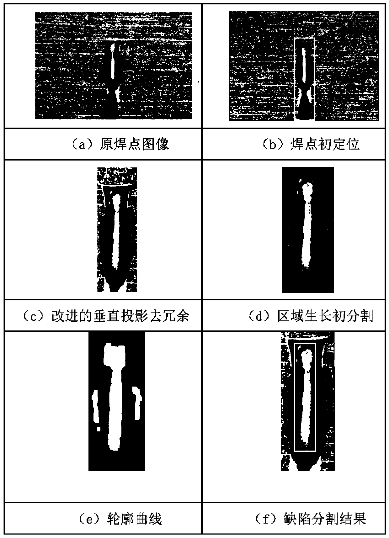
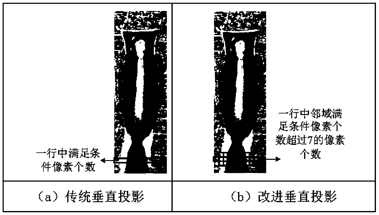
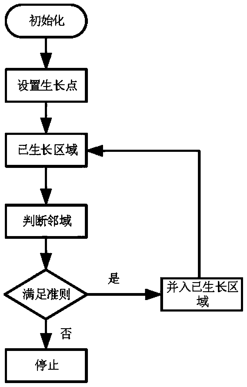
[0042] see Figure 1-Figure 8 , a method for locating and classifying defects in wire bonding solder joints provided in this embodiment, comprising the following steps:
[0043] (1) Use an industrial camera to obtain images of bonded solder joints; pre-purchase an ultrasonic bonding platform. The hardware of the ultrasonic bonding platform consists of a basic structure and a force feedback structure. The basic structure includes an ultrasonic generation subsystem and a motion control subsystem. It is composed of a visual subsystem, and the force feedback structure obtains the bonding pressure in real time through the force sensor and provides corresponding feedback. The control software of the ultrasonic bonding platform includes the following parts: motion control part, ultrasonic driver control part, image display and positioning part, light source control part and force control part. The ultrasonic driver in the ultrasonic generation subsystem is a low-power ultrasonic gen...
PUM
 Abstract
Description
Claims
Application Information