Image sensor and formation method thereof

A technology of image sensor and curved surface structure, which is applied in the direction of electric solid-state devices, semiconductor devices, electrical components, etc., can solve the problem of optical crosstalk that needs to be improved, and achieve the effects of reducing reflection, improving efficiency, and reducing light crosstalk

Inactive Publication Date: 2019-11-01
HUAIAN IMAGING DEVICE MFGR CORP
View PDF3 Cites 3 Cited by
  • Summary
  • Abstract
  • Description
  • Claims
  • Application Information

AI Technical Summary

Problems solved by technology

[0005] However, in the prior art, the problem of optical crosstalk still needs to be improved

Method used


Image

  • Image sensor and formation method thereof
  • Image sensor and formation method thereof
  • Image sensor and formation method thereof

Examples


Embodiment Construction

[0029] In the existing image sensor technology, the optical signal passes through the lens module to the lens structure for focusing, and then passes through the filter to reach the independent pixel (for example, including a photodiode) for photoelectric conversion. Among them, when the lens structure captures the incident light, it is filtered by the filter structure to remove irrelevant light and form monochromatic light. The incident photons reach the semiconductor substrate and are absorbed by the pixel device to generate photogenerated carriers to output electrical signals. However, in the prior art, the problem of optical crosstalk still needs to be improved.

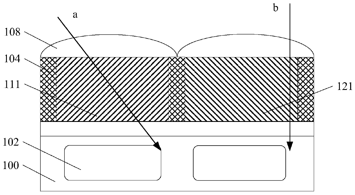
[0030] refer to figure 1 , figure 1 It is a schematic diagram of a device cross-sectional structure of an image sensor in the prior art.

[0031] In an existing image sensor, a semiconductor substrate 100 may be provided, grid structures 104 are formed on the surface of the semiconductor substrate 100, color fi...


PUM


Abstract

The present invention provides an image sensor and a formation method thereof. The image sensor comprises: a semiconductor substrate; a convex lens located on the surface of the semiconductor substrate; and a convex transparent surface structure located on the surface of the convex lens, wherein the upper and lower surfaces of the convex transparent surface structure are curved surfaces, and the radius of curvature of the upper surface is smaller than that of the radius of curvature of the lower surface, the upper surface of the convex transparent surface structure is a surface far away from the semiconductor substrate, and the lower surface of the convex transparent surface structure is a surface close to the semiconductor substrate. According to the scheme, the image sensor and the formation method thereof facilitate reduction of light crosstalk and improvement of the efficiency of photoelectric conversion.

Description

technical field [0001] The invention relates to the technical field of semiconductor manufacturing, in particular to an image sensor and a forming method thereof. Background technique [0002] The image sensor is the core component of the camera equipment, which realizes the image capture function by converting the optical signal into an electrical signal. Taking a CMOS image sensor (CMOS Image Sensors, CIS) device as an example, due to its advantages of low power consumption and high signal-to-noise ratio, it has been widely used in various fields. [0003] Taking Back-side Illumination (BSI) CIS as an example, in the existing manufacturing process, logic devices and pixel devices are first formed in the semiconductor substrate and metal interconnection structures are formed on the surface of the semiconductor substrate, and then Bonding the carrier wafer with the front side of the semiconductor substrate, and then thinning the back of the semiconductor substrate, and then...

Claims


Application Information

Patent Timeline
Patent Type & Authority Applications(China)
IPC IPC(8): H01L27/146
CPCH01L27/14627H01L27/14685
Inventor 吴明郭松辉林宗贤孙明亮朱晓彤
Owner HUAIAN IMAGING DEVICE MFGR CORP
Why Eureka
Try Eureka