Flexible printed circuit board and manufacturing method thereof

A flexible printing and circuit board technology, applied in printed circuit manufacturing, printed circuits, printed circuits, etc., can solve the problems of tin-copper alloy layer disconnection, increase manufacturing cost, disconnection reliability, etc., and achieve enhanced bending performance. , The effect of preventing the generation of voids and reducing the manufacturing cost

A flexible printing and circuit board technology, applied in printed circuit manufacturing, printed circuits, printed circuits, etc., can solve the problems of tin-copper alloy layer disconnection, increase manufacturing cost, disconnection reliability, etc., and achieve enhanced bending performance. , The effect of preventing the generation of voids and reducing the manufacturing cost

CN110402020AActive Publication Date: 2019-11-01江苏上达半导体有限公司

Image

  • Flexible printed circuit board and manufacturing method thereof
  • Flexible printed circuit board and manufacturing method thereof
  • Flexible printed circuit board and manufacturing method thereof

Examples


Embodiment 1

[0034] A method for manufacturing a flexible printed circuit board, the steps comprising:

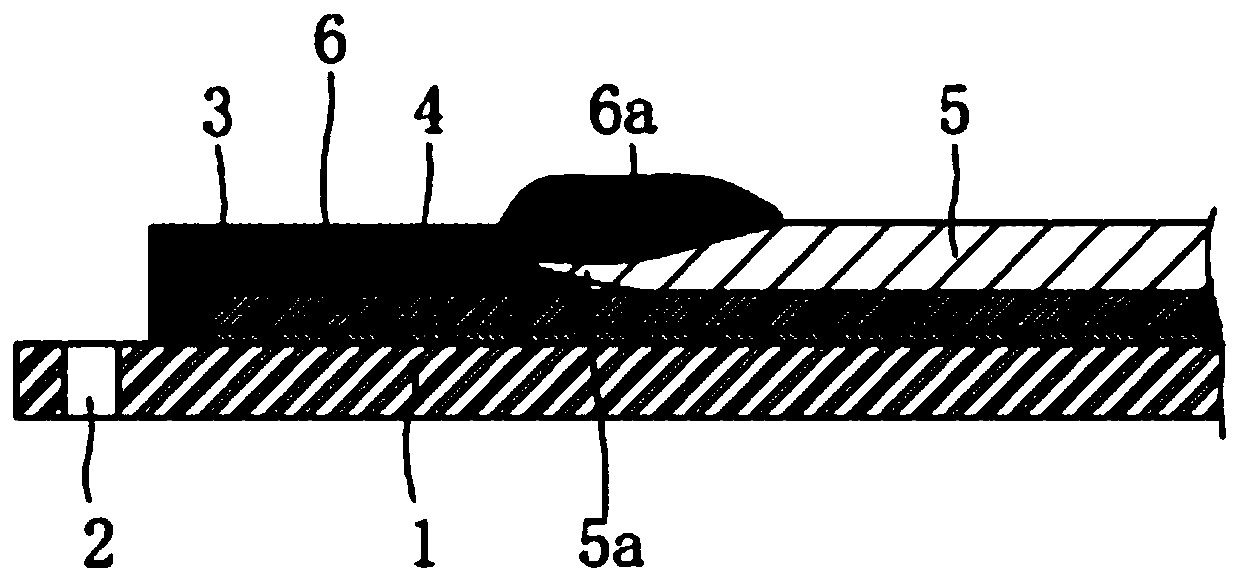
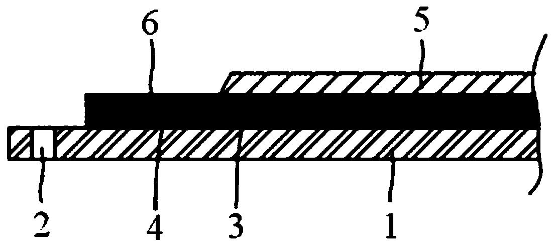
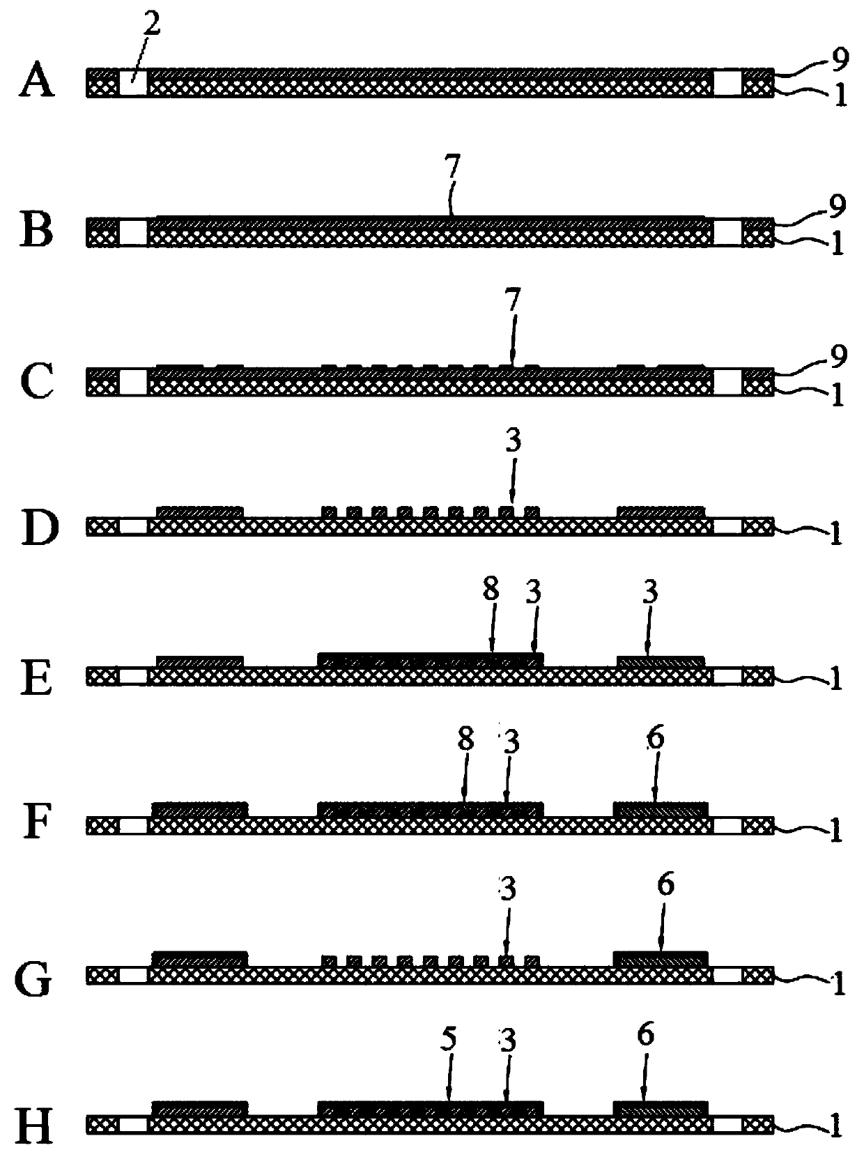
[0035] First, apply an adhesive 4 on one side of the flexible and insulating plastic film-like insulating substrate 1, and use the adhesive 4 to press the conductor layer 9 on the insulating substrate 1. The conductor used here is preferably copper foil, and the insulation The general thickness of the substrate 1 is 12.5-50 μm, and then the sprocket holes 2 are punched continuously at certain intervals using a mold;

[0036] Then, as the traditional processing method, after the photoresist 7 is coated on the surface of the conductor, the conductor pattern 3 is formed by exposure and etching, and the unnecessary photoresist is removed with an alkaline liquid. Inner pins 3a of semiconductors, outer pins 3b for connection to other printed circuit boards or electronic components, etc., and plating leads used in electrolytic plating, etc.;

[0037] Next, in order to protect the conductor pa...


PUM


Abstract

The invention discloses a flexible printed circuit board. The flexible printed circuit board comprises an insulation substrate, the insulation substrate is provided with a conductor layer, the insulation substrate is punched with a sprocket hole by adopting a die, and the flexible printed circuit board further comprises an electroplated tin alloy layer, a solder resist and a resist; the conductorlayer is etched to form a conductor pattern, the part in the conductor pattern except a connecting terminal is printed with the resist; the connecting terminal in the conductor pattern is provided with the electroplated tin alloy layer; and when the resist printed in the conductor pattern is peeled off, the solder resist is printed at the same position. The connecting terminal on the circuit pattern except the connecting terminal is printed with the layer of solder resist, then the connecting terminal in the conductor pattern is provided with the electroplated tin alloy layer, and after the resist is peeled off, the solder resist is printed, so that there is no a tin layer at the lower portion of the solder resist to avoid the heat treatment during printing of the solder resist to diffusethe copper into the tin layer to form a fragile tin-copper alloy layer to improve the bending properties of the product.

Description

technical field [0001] The invention relates to a flexible printed circuit board and a manufacturing method thereof, belonging to the technical field of electronic components. Background technique [0002] In recent years, with the rapid development of the electronics industry, electronic devices have become thinner, smaller, lighter, and shorter, followed by high-density and high-precision requirements for circuit patterns on circuit boards. At present, it is generally used to form circuit patterns on flexible and insulating films such as polyimide, such as figure 1 As shown, using a plastic film-like insulating substrate 1 with flexibility and insulating properties, the adhesive 4 is coated on the insulating substrate 1, and the copper foil is laminated with the adhesive 4 to form a conductor layer; or by sputtering and electroplating, A copper foil conductor layer is formed on the insulating substrate layer, and the insulating substrate layer and the copper foil conducto...

Claims


Application Information

Patent Timeline
01 Nov 2019
Publication
CN110402020A
IPC
H05K1/02; H05K1/11; H05K3/28
CPC
H05K1/028; H05K1/118; H05K3/282; H05K2201/2009
Inventors
黄春生; 杨洁