Etching device for manufacturing semiconductor chip and use method thereof

An etching device and semiconductor technology, applied in semiconductor/solid-state device manufacturing, transportation and packaging, conveyor objects, etc., can solve problems such as low work efficiency, achieve the effect of improving yield rate, avoiding excessive etching, and improving reaction rate

Pending Publication Date: 2019-11-05
NANJING COLLEGE OF INFORMATION TECH
View PDF0 Cites 2 Cited by
  • Summary
  • Abstract
  • Description
  • Claims
  • Application Information

AI Technical Summary

Problems solved by technology

[0003] But generally during etching process, after the semiconductor board is reacted in the reaction solution, if the reaction solution is not cleaned up in time, excessive etching will occur, which will seriously increase the defective rate, and after cleaning, it is necessary to clean it. If ordinary air drying is used, the work efficiency will be lower

Method used


Image

  • Etching device for manufacturing semiconductor chip and use method thereof
  • Etching device for manufacturing semiconductor chip and use method thereof
  • Etching device for manufacturing semiconductor chip and use method thereof

Examples


Embodiment 1

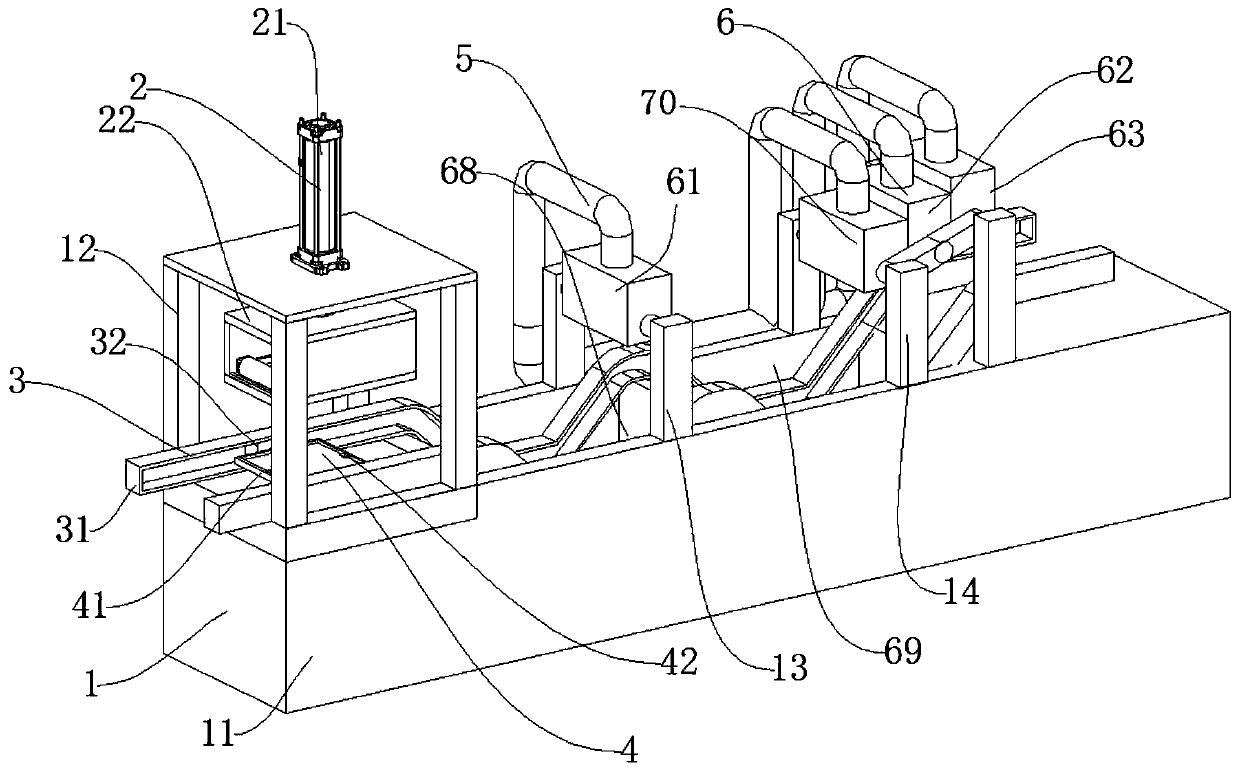
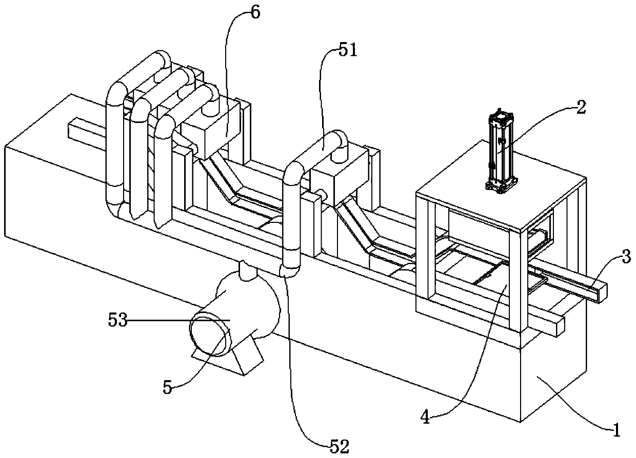
[0040] Embodiments of the present invention provide an etching device for manufacturing semiconductor chips, such as Figure 1-2 As shown, it specifically includes a support mechanism 1, a transport mechanism 3, a printing mechanism 2, an air supply mechanism 5 and a reaction mechanism 6;

[0041] The supporting mechanism 1 plays a supporting role;

[0042] The transport mechanism 3 is connected to the support mechanism 1, and is used to drive the circuit board to be etched to move along a preset track;

[0043] The printing mechanism 2, the air supply mechanism 5 and the reaction mechanism 6 are arranged in sequence, and all three are arranged above the transportation mechanism 3; the printing mechanism 2 plays a printing role; the air supply mechanism 5 is used to provide air source, the output end of which is connected to the input end of the reaction mechanism 6. When the circuit board moves below the reaction mechanism 6, the gas supply mechanism 5 provides high-pressure...

Embodiment 2

[0061] In the embodiment of the present invention, it is proposed to increase the reaction rate of the whole device by increasing the boiling efficiency of the reaction liquid and the cleaning liquid (water). Based on Embodiment 1, in the embodiment of the present invention, the reaction liquid tank 68 and the water tank 69 Stirring mechanism 7 is arranged inside, and described stirring mechanism 7 comprises stirring motor 71, connecting shaft 72 and stirring seat 73; Described stirring motor 71 links to each other with described stirring seat 73 by described connecting shaft 72, during specific implementation, The connecting shaft 72 is connected to the stirring motor 71 through a coupling, and the effective transmission of force is ensured through the connection of the coupling. For details, see Figure 8 .

Embodiment 3

[0063] An embodiment of the present invention provides a method for using an etching device for semiconductor chip manufacturing, including:

[0064] Place the circuit board to be etched on the transport mechanism 3;

[0065] The transportation mechanism 3 drives the circuit board to be etched to move to the bottom of the printing mechanism 2, and the printing mechanism 2 applies the dressing on the circuit board;

[0066] When the transport mechanism 3 drives the circuit board to move below the reaction mechanism 6, the gas supply mechanism 5 supplies high-pressure gas to the reaction mechanism 6, and the reaction mechanism 6 blows air to the circuit board.

[0067] More specifically, when the method for using the etching device for manufacturing semiconductor chips in this embodiment is applied to the device in Embodiment 1, the following steps are specifically included:

[0068] a, the circuit board that needs to be etched is placed in the groove on the transport plate 41,...


PUM


Abstract

The invention discloses an etching device for manufacturing a semiconductor chip and a use method thereof. The etching device comprises a supporting mechanism, a transporting mechanism, a printing mechanism, a gas supply mechanism and a reaction mechanism. The transporting mechanism is connected with the supporting mechanism and used for driving a circuit board to be etched to move along a presettrajectory. The printing mechanism, the gas supply mechanism and the reaction mechanism are sequentially arranged, and are all arranged above the transporting mechanism. The output end of the gas supply mechanism is connected with the input end of the reaction mechanism. When the circuit board moves below the reaction mechanism, the gas supply mechanism supplies high pressure gas to the reaction mechanism, and the reaction mechanism blows gas to the circuit board. According to the invention, the transporting mechanism is used to drive the circuit board to move along the preset trajectory; thecircuit board is printed by using the printing mechanism; the gas supply mechanism supplies high pressure gas to the reaction mechanism; when the circuit board moves to the reaction mechanism, the circuit board is cleaned by the high pressure gas; excessive etching of reaction liquid is avoided; and the yield is greatly improved.

Description

technical field [0001] The invention belongs to the field of semiconductor chip manufacturing, and in particular relates to an etching device for semiconductor chip manufacturing and a using method thereof. Background technique [0002] Etching is the technique of removing material using chemical reaction or physical impact. Etching techniques can be classified into wet etching and dry etching. It can be used to make copper plates, zinc plates and other printing concave-convex plates at the earliest, and it is also widely used in the processing of weight-reducing instrument panels, nameplates and thin workpieces that are difficult to process by traditional processing methods; after continuous improvement and development of process equipment, it can also be used It is used in the processing of precision etching products of thin electronic parts in aviation, machinery, and chemical industries. Especially in semiconductor manufacturing processes, etching is an indispensable te...

Claims


Application Information

Patent Timeline
Patent Type & Authority Applications(China)
IPC IPC(8): H01L21/67H01L21/677
CPCH01L21/67011H01L21/67023H01L21/67034H01L21/67075H01L21/67742
Inventor 李建林张永武文扬
Owner NANJING COLLEGE OF INFORMATION TECH
Why Eureka
Try Eureka