Automatic packaging system and method for electronic components

A technology for electronic components and automatic packaging, applied in the field of chip manufacturing, can solve the problems of low efficiency and high labor costs, and achieve the effect of reducing production costs and improving packaging efficiency

Active Publication Date: 2021-10-12
SUZHOU TF AMD SEMICON CO LTD
View PDF6 Cites 0 Cited by
  • Summary
  • Abstract
  • Description
  • Claims
  • Application Information

AI Technical Summary

Problems solved by technology

[0006] In addition to the semi-automatic cable tie packing machine, vacuum heat sealing machine and other equipment, other operations such as traying, bagging, carton forming, wrapping cushioning materials, boxing, sealing and labeling are completely dependent on manual labor. Operation, low efficiency, high labor cost

Method used


Image

  • Automatic packaging system and method for electronic components
  • Automatic packaging system and method for electronic components
  • Automatic packaging system and method for electronic components

Examples


Embodiment Construction

[0084] The packaging system and packaging method provided by the present invention will be further described in detail below in conjunction with the accompanying drawings and embodiments.

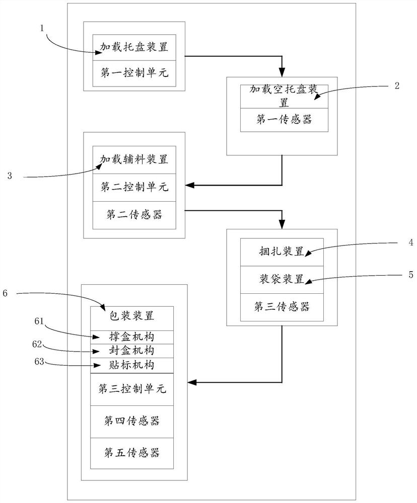
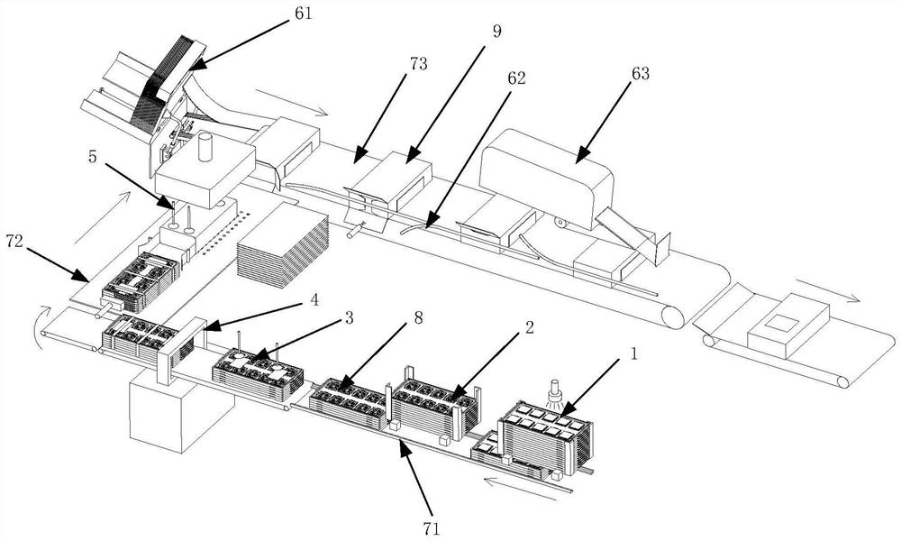
[0085] refer to figure 1 , a flowchart of a packaging system according to an embodiment of the present invention. refer to figure 2 , the packaging system includes a tray loading device 1, a first control unit, an auxiliary material loading device 3, a second control unit, a second sensor, a packaging device 6, a third control unit, a fourth sensor and a fifth sensor.

[0086] The pipelines include a first pipeline 71 , a second pipeline 72 and a third pipeline 73 . The loading tray device 1 is correspondingly arranged on the first assembly line 71 , the auxiliary material adding device 3 is correspondingly arranged on the second assembly line 72 , and the packaging device 6 is correspondingly arranged on the third assembly line 73 .

[0087] The first control unit can control the loadi...


PUM


Abstract

The invention discloses an automatic packaging system and method for electronic components. The system includes: a loading tray device and a first control unit arranged on a first assembly line; an auxiliary material loading device, a second control unit and a first control unit arranged on a second assembly line The second sensor is arranged on the packaging device of the third assembly line, the third control unit, the fourth sensor and the fifth sensor. The invention can meet the requirements of production automation, is beneficial to improving the packaging efficiency of electronic products and reducing production costs.

Description

technical field [0001] The invention relates to the field of chip manufacturing, in particular to a packaging system and method for electronic components. Background technique [0002] As a high-end manufacturing industry, chip manufacturing has achieved intelligence and automation in most of the processes, with high production efficiency. However, the packaging process is an essential process in the back-end process of chip manufacturing, especially in the chip packaging and testing industry. Packaging efficiency restricts the efficiency improvement and cost saving of chip manufacturing to a certain extent. [0003] At present, the chip manufacturing industry needs to rely on manual packaging operations due to the following reasons: [0004] 1. The aircraft box-shaped packaging box has a complex structure and requires manual folding and sealing. [0005] 2Separate out several trays of chips according to the specified packaging quantity, manually add an empty tray on top o...

Claims


Application Information

Patent Timeline
Patent Type & Authority Patents(China)
IPC IPC(8): B65B65/00B65B57/00B65B35/10B65B61/20B65B31/02B65B51/14B65B43/30B65B43/36B65B5/06B65B43/18B65B43/26B65B51/02B65G59/06
CPCB65B5/06B65B31/024B65B35/10B65B43/185B65B43/26B65B43/30B65B43/36B65B51/023B65B51/146B65B57/00B65B61/20B65B61/202B65B65/003B65B2220/18B65G59/067
Inventor 边兵兵焦洁王港善郭瑞亮
Owner SUZHOU TF AMD SEMICON CO LTD
Why Eureka
Try Eureka