Unlock instant, AI-driven research and patent intelligence for your innovation.

Kit and reaction chamber

A reaction chamber and process technology, applied in metal material coating process, ion implantation plating, coating and other directions, can solve the problems of poor particle control effect, insufficient roughness, large damage to the process kit, etc., to improve the service life , the effect of increasing roughness and reducing stress

Active Publication Date: 2019-11-19
BEIJING NAURA MICROELECTRONICS EQUIP CO LTD +1
View PDF8 Cites 0 Cited by
  • Summary
  • Abstract
  • Description
  • Claims
  • Application Information

AI Technical Summary

Problems solved by technology

However, grit blasting did not produce enough roughness to improve process kit life significantly and particle control was poor
As for the spraying treatment, although the roughness can be increased to a certain extent, the spraying treatment has relatively large damage to the process kit, which reduces the number of cycles of the process kit

Method used


Image

  • Kit and reaction chamber
  • Kit and reaction chamber
  • Kit and reaction chamber

Examples


Embodiment Construction

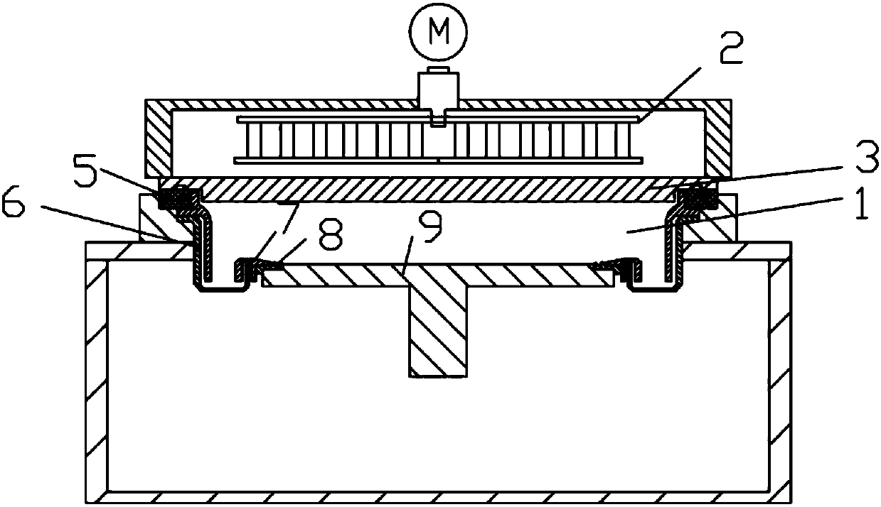
[0040] In order for those skilled in the art to better understand the technical solution of the present invention, the process kit and the reaction chamber provided by the present invention will be described in detail below with reference to the accompanying drawings.

[0041] The surface of the process kit provided by the present invention is provided with a textured structure, and the pattern structure is used to increase the roughness of the surface of the process kit so as to control particles.

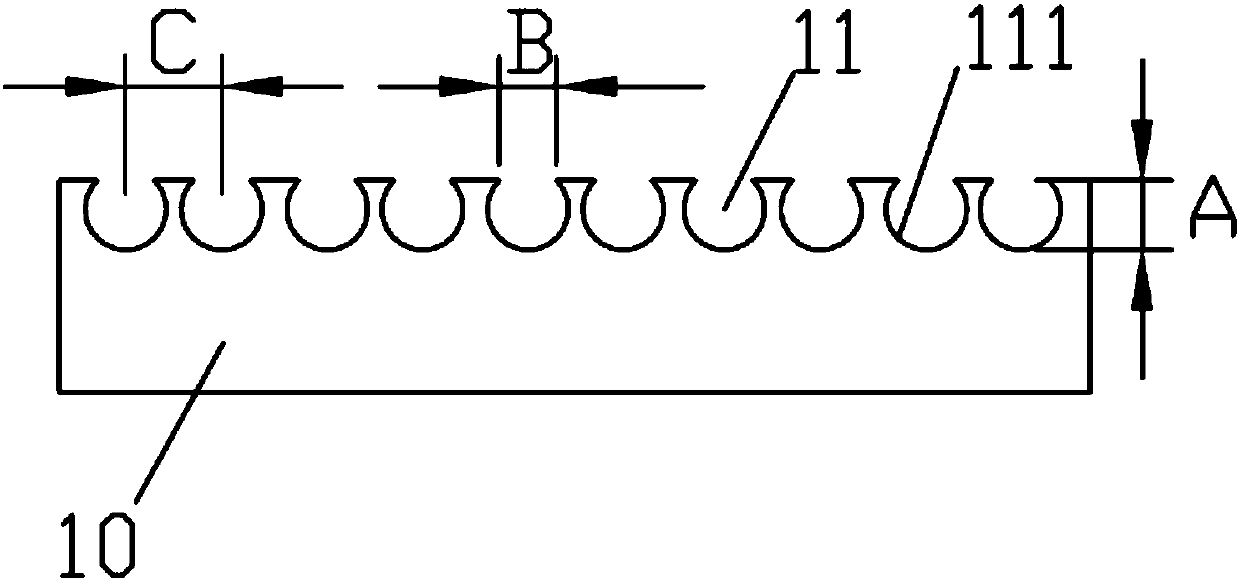
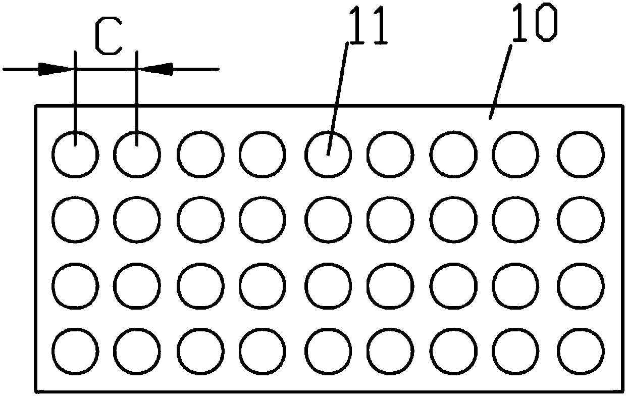
[0042] Please also refer to Figure 2A to Figure 2B , in the process kit provided in the first embodiment of the present invention, the textured structure 10 includes a plurality of recesses 11 , and each recess 11 includes a spherical concave surface 111 .

[0043] The roughness of the surface of the process kit can be increased by means of multiple recesses 11 , and the roughness of this structure can reach Ra40-60. At the same time, with the help of the spherical concave surfa...


PUM


Abstract

The invention provides a kit and a reaction chamber. A pattern structure is arranged on the surface of the kit, and the pattern structure comprises a plurality of concave parts, wherein each concave part comprises a spherical concave surface. The pattern structure not only can effectively improve particle control effect, but also cannot cause injury to the surface of the kit, thereby prolonging use life of the kit.

Description

technical field [0001] The invention relates to the technical field of semiconductor manufacturing, in particular to a process kit and a reaction chamber. Background technique [0002] Physical Vapor Deposition (PVD, Physical Vapor Deposition) technology or sputtering (Sputtering) deposition technology is the most widely used thin film manufacturing technology in the semiconductor industry. Physical vapor deposition technology can be applied to many process fields, such as copper interconnection technology, through silicon via (ThroughSiliconVia, TSV) technology in the packaging field, and so on. [0003] With the continuous development of semiconductor technology, the size of integrated circuits is getting smaller and smaller, and Low-k materials appear in the interconnection process. In order to obtain a better etching morphology and protect the Low-k material to a certain extent, a TiN film is deposited on the Low-k material as a metal hard mask for etching the Low-k mat...

Claims


Application Information

Patent Timeline
IPC IPC(8): C23C14/50C23C14/35
CPCC23C14/50C23C14/35
Inventor 刘建强白志民邱国庆李强邓斌王厚工丁培军张兴
Owner BEIJING NAURA MICROELECTRONICS EQUIP CO LTD
Features
  • R&D
  • Intellectual Property
  • Life Sciences
  • Materials
  • Tech Scout
  • Unparalleled Data Quality
  • Higher Quality Content
  • 60% Fewer Hallucinations
Learn More