Method for filling electroplated copper

A process method and technology for electroplating copper, which are applied in the manufacturing of circuits, electrical components, semiconductor/solid-state devices, etc., can solve the problems of increasing the difficulty of the filling process of electroplating copper, reduce the difficulty of filling, improve the filling quality, and increase the Q-Time window. Effect

Inactive Publication Date: 2019-11-19
SHANGHAI HUALI INTEGRATED CIRCUTE MFG CO LTD
View PDF2 Cites 2 Cited by
  • Summary
  • Abstract
  • Description
  • Claims
  • Application Information

AI Technical Summary

Problems solved by technology

In the presence of copper oxide 105, the electroplating solution of the copper electroplating process, especially the acidic electroplating solution such as sulfuric acid, can quickly dissolve the copper seed crystal layer 104 formed with copper oxide 105 on the surface, such as Figure 1C At the position of the bottom corner of the trench or via hole 102 corresponding to the mark 202, the thickness of the copper seed layer 104 itself is relatively thin, and a weak point (weak point) will be generated after being rapidly dissolved, which will increase the electroplating copper filling process. difficulty

Method used


Image

  • Method for filling electroplated copper
  • Method for filling electroplated copper
  • Method for filling electroplated copper

Examples


Embodiment Construction

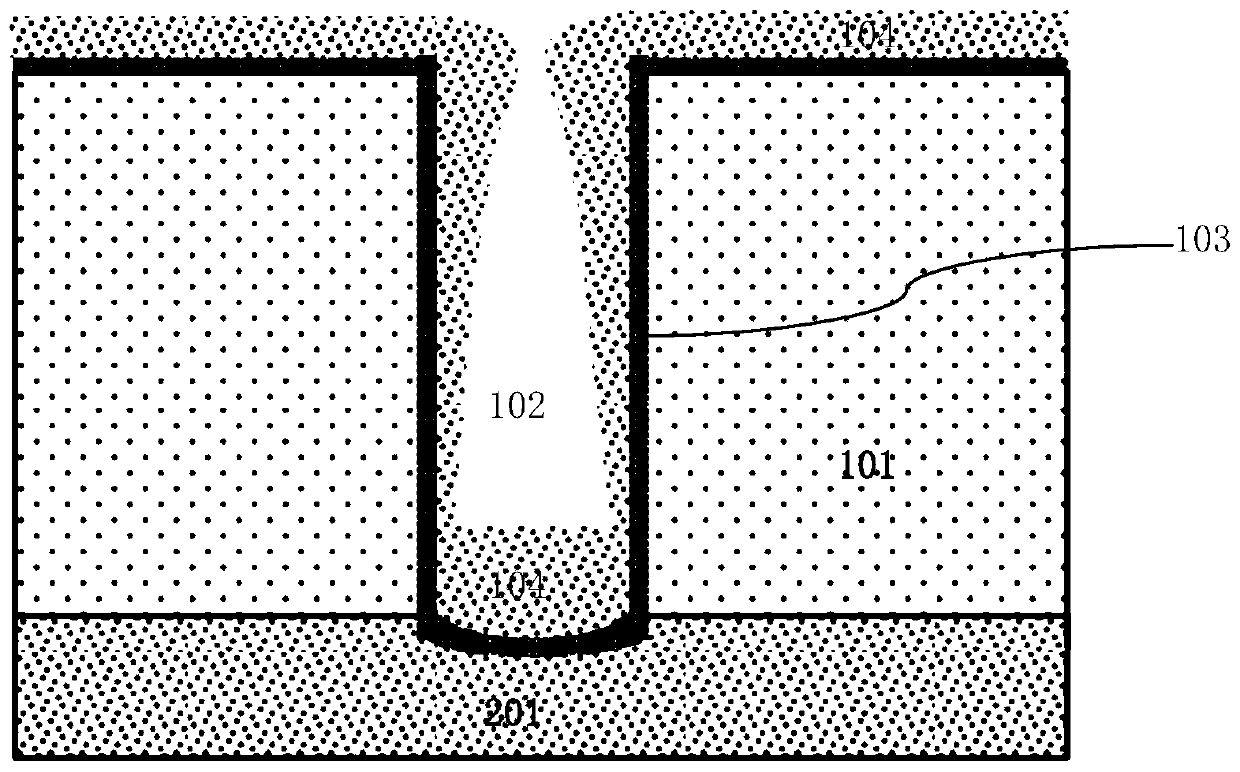
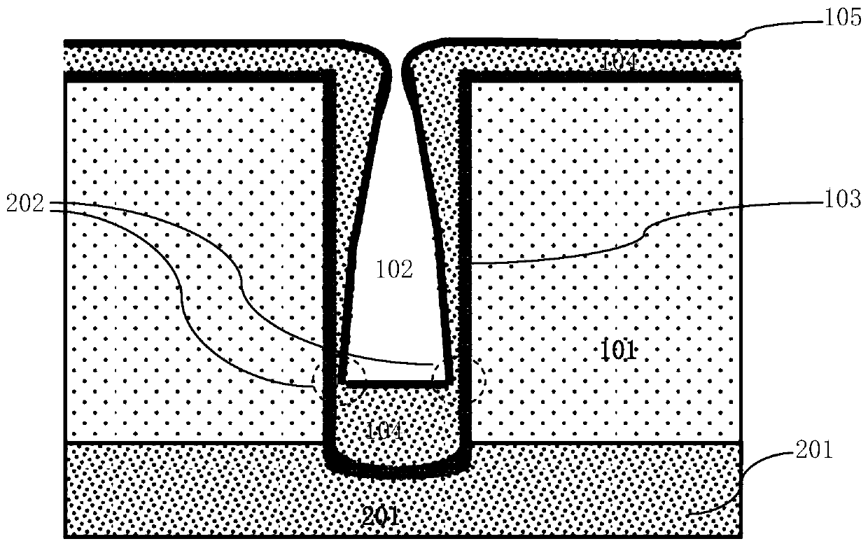
[0045] Such as figure 2 Shown is the flow chart of the electroplating copper filling process method of the embodiment of the present invention; as Figure 3A to Figure 3D As shown, it is a device structure diagram in each step of the electroplating copper filling process method of the embodiment of the present invention. The electroplating copper filling process method of the embodiment of the present invention includes the following steps:

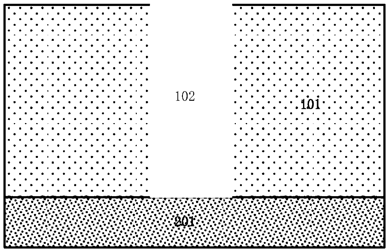
[0046] Step one, such as Figure 3A As shown, trenches or vias 102 are formed.

[0047] Preferably, the trench or via hole 102 is formed in the interlayer film 101 . In other embodiments, the trench or via hole 102 can also be directly formed in a semiconductor substrate such as a silicon substrate.

[0048] The trench or via hole 102 is formed by photolithography definition plus etching process.

[0049] The etching process for forming the trench or the through hole 102 is dry etching.

[0050] Step two, such as Figure 3B As show...


PUM


Abstract

The invention discloses a method for filling electroplated copper, comprising the steps of 1, forming a trench or a through hole; 2, forming a copper seed crystal layer on the inner surface of the trench or the via hole; 3, oxidizing the surface of the copper seed crystal layer to form copper oxide during the waiting time between the formation of the copper seed crystal layer and the copper electroplating process in the next step; 4, performing a reduction process before the copper electroplating process, and then performing the copper electroplating process to fill the trench or the through hole with the copper layer. The method, by performing the reduction process before the copper electroplating process, can eliminate the copper oxide on the surface of the copper seed crystal layer during the copper electroplating process and keep the thickness of the copper seed crystal layer at various positions on the inner surface of the trench or the through hole, thereby reducing the difficulty of the electroplated copper filling process and improving the electroplated copper filling ability.

Description

technical field [0001] The invention relates to a manufacturing method of a semiconductor integrated circuit, in particular to an electroplating copper filling process method. Background technique [0002] Such as Figure 1A to Figure 1C As shown, it is a device structure diagram in each step of the existing electroplating copper filling process method, and the existing electroplating copper filling process method includes the following steps: [0003] Step one, such as Figure 1A As shown, trenches or vias 102 are formed. [0004] Typically, the trench or via hole 102 is formed in the interlayer film 101 . [0005] The trench or via hole 102 is formed by photolithography definition plus etching process. [0006] The etching process for forming the trench or the through hole 102 is dry etching. [0007] Step two, such as Figure 1B As shown, a copper diffusion barrier layer 103 and a copper seed layer 104 are sequentially formed on the inner surface of the trench or via...

Claims


Application Information

Patent Timeline
Patent Type & Authority Applications(China)
IPC IPC(8): H01L21/768
CPCH01L21/76879H01L21/76838H01L21/76843H01L21/76873H01L21/76861H01L21/7684H01L21/76856H01L21/76874
Inventor 王俊杰陈建勋蔡旻錞
Owner SHANGHAI HUALI INTEGRATED CIRCUTE MFG CO LTD
Why Eureka
Try Eureka