In-situ heating chip and manufacturing method thereof

A heating chip, in-situ technology, used in ion implantation plating, coating, instruments, etc., can solve the problems of in-situ chip being unable to apply external thermal field, online observation sample drift, and uneven heating, etc., to achieve stable observation of samples. position, guaranteed uniformity and temperature stability, easy operation effect

Inactive Publication Date: 2019-11-26
XIAMEN CHIP NOVA TECH CO LTD
View PDF7 Cites 6 Cited by
  • Summary
  • Abstract
  • Description
  • Claims
  • Application Information

AI Technical Summary

Problems solved by technology

[0004] The invention provides an in-situ heating chip and a manufacturing method thereof, the purpose of which is to realize the integrated design of the in-situ heating chip, and at the same time solve the problem that the in-situ chip cannot be applied with an external thermal field or the heating is uneven, which leads to serious drift of the online observation sample question

Method used


Image

  • In-situ heating chip and manufacturing method thereof
  • In-situ heating chip and manufacturing method thereof
  • In-situ heating chip and manufacturing method thereof

Examples


Embodiment Construction

[0040]In order to enable those skilled in the art to better understand the solutions of the present invention, the technical solutions in the embodiments of the present invention will be clearly and completely described below in conjunction with the drawings in the embodiments of the present invention. The described embodiments are only some, not all, embodiments of the present invention. Based on the embodiments of the present invention, all other embodiments obtained by persons of ordinary skill in the art without making creative efforts shall fall within the protection scope of the present invention. The following examples are intended to illustrate the present invention, but should not be construed as limiting the present invention. Any equivalent replacement technical solutions are within the protection scope of the present invention.

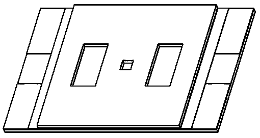
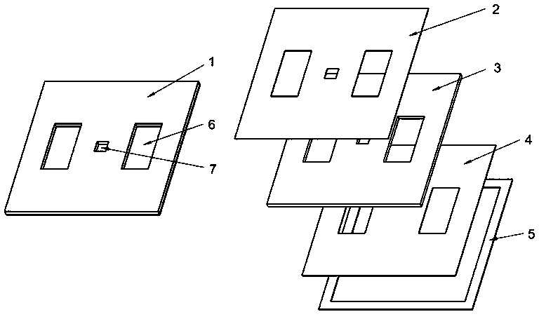
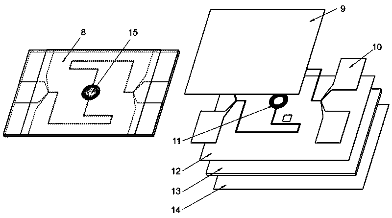
[0041] The embodiment of the present invention discloses an in-situ heating chip, such as figure 1 , figure 2 , image 3 As shown, i...


PUM

PropertyMeasurementUnit
thicknessaaaaaaaaaa
thicknessaaaaaaaaaa
thicknessaaaaaaaaaa

Abstract

The invention discloses an in-situ heating chip and a manufacturing method thereof. The in-situ heating chip comprises a first substrate and a second substrate. The first substrate is manufactured byusing a silicon substrate, a silicon nitride thin film and a metal bonding layer. The second substrate is manufactured by using a silicon substrate, a silicon nitride thin film, a four-electrode system and a heating metal wire. The first substrate and the second substrate are sequentially arranged from top to bottom. The first substrate is provided with two symmetrical liquid injection ports and aviewing window. The second substrate is provided with a central viewing window. The viewing window of the first substrate and the central viewing window of the second substrate are vertically alignedand consistent in size, and are bonded by means of the metal bonding layer to realize the integrated in-situ heating chip. The invention further discloses a manufacturing method of the in-situ heating chip. The in-situ heating chip enables the user to achieve the purposes of heating the sample while observing the same, ensures the atomic-scale resolution, and obviously expands the application field of electron microscope observation by introducing a thermal field.

Description

technical field [0001] The invention belongs to the field of in-situ characterization, and in particular relates to an in-situ heating chip and a manufacturing method thereof. Background technique [0002] In situ transmission electron microscopy is widely used in various scientific fields due to its advantages of ultra-high spatial resolution (atomic level) and ultra-fast time resolution (millisecond level), which provides researchers with the opportunity to explore the microstructure of new materials. New ideas and research methods. The main performance is to build a visual window in the electron microscope, introduce external field effects such as thermal field, light field, electrochemical field, etc., and perform real-time dynamic in-situ testing on the sample. Researchers can use in-situ testing technology to capture the dynamic response of samples to the environment, including important information such as size, shape, crystal structure, atomic structure, chemical ke...

Claims


Application Information

Patent Timeline
Patent Type & Authority Applications(China)
IPC IPC(8): G01N23/2202G01N23/2251C23C14/16C23C14/24C23C14/30C23C14/04
CPCC23C14/042C23C14/16C23C14/24C23C14/30G01N23/2202G01N23/2251G01N2223/07G01N2223/102G01N2223/3106H01J37/20H01J2237/2003
Inventor 廖洪钢
Owner XIAMEN CHIP NOVA TECH CO LTD
Why Eureka
Try Eureka