Organic material and perovskite material combination-based full-solution flexible white-light device and fabrication method thereof
A technology of perovskite materials and organic materials, applied in semiconductor/solid-state device manufacturing, electric solid-state devices, semiconductor devices, etc., can solve the problems of complex process and expensive manufacturing cost, and achieve simplified preparation process, high color rendering index, The effect of promoting efficient transmission
- Summary
- Abstract
- Description
- Claims
- Application Information
AI Technical Summary
Problems solved by technology
Method used
Image

Examples
Embodiment 1
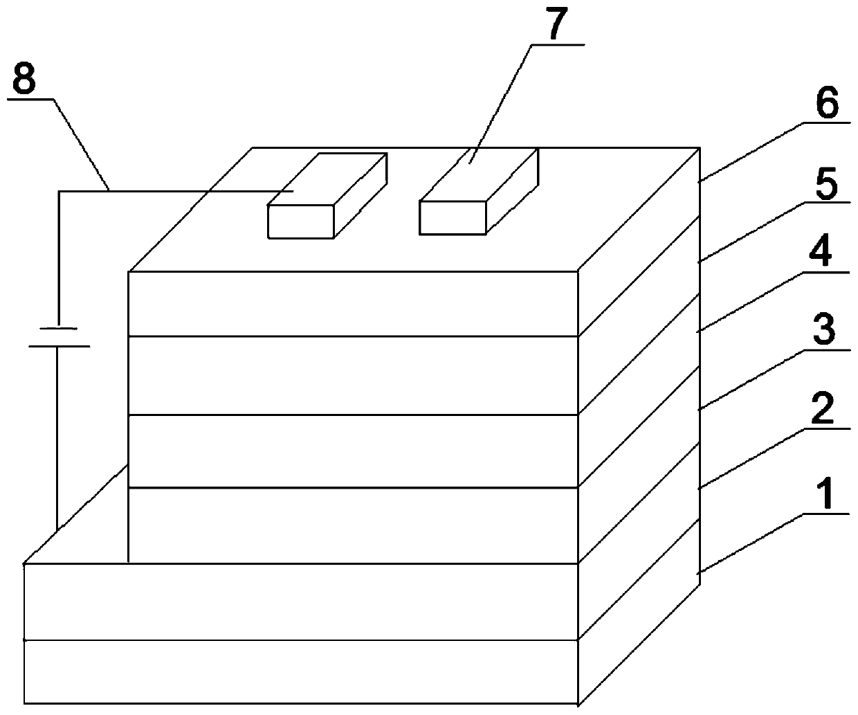
[0034] like figure 1 As shown, the all-solution flexible white light device based on the combination of organic materials and perovskite materials and its preparation method, the white light device shown from bottom to top are flexible substrate 1, anode 2, hole transport layer 3, blue light active Layer I (serving as a hole buffer layer at the same time) 4, perovskite red light-emitting layer II5, and organic green photoactive layer III (serving as an electron buffer layer at the same time) 6, cathode 7, and driving voltage 8. Wherein, the anode 2 is located on the surface of the flexible substrate 1 , and the white light device emits light under the drive of an external power source 8 .
[0035] The white light device structure from top to bottom is as follows:
[0036] PI-substrate / ITO / PEDOT:PSS(20nm) / TFB(5nm) / CsPbl 3 (10nm) / Alq 3 (5nm) / Ag(100nm)
[0037] The preparation method is:
[0038] Step 1: Spin-coat the hole transport layer PEDOT:PSS on the dry flexible substr...
Embodiment 2
[0045] like figure 1 As shown, the all-solution flexible white light device based on the combination of organic materials and perovskite materials and its preparation method, the white light device shown from bottom to top are flexible substrate 1, anode 2, hole transport layer 3, blue light active Layer I (serving as a hole buffer layer at the same time) 4, perovskite red light-emitting layer II5, and organic green photoactive layer III (serving as an electron buffer layer at the same time) 6, cathode 7, and driving voltage 8. Wherein, the anode 2 is located on the surface of the flexible substrate 1 , and the white light device emits light under the drive of an external power source 8 .
[0046] The white light device structure from bottom to top is as follows:
[0047] PI-substrate / ITO / PEDOT:PSS(20nm) / PTAA(5nm) / CsPbl 3 (20nm) / Alq 3 (5nm) / Ag(100nm)
[0048] The preparation method is:
[0049] Step 1: Spin-coat the hole transport layer PEDOT:PSS on the dry flexible subst...
Embodiment 3
[0056] like figure 1 As shown, the all-solution flexible white light device based on the combination of organic materials and perovskite materials and its preparation method, the white light device shown from bottom to top are flexible substrate 1, anode 2, hole transport layer 3, blue light active Layer I (serving as a hole buffer layer at the same time) 4, perovskite red light-emitting layer II5, and organic green photoactive layer III (serving as an electron buffer layer at the same time) 6, cathode 7, and driving voltage 8. Wherein, the anode 2 is located on the surface of the flexible substrate 1 , and the white light device emits light under the drive of an external power source 8 .
[0057] The white light device structure from bottom to top is as follows:
[0058] PI-substrate / ITO / PEDOT:PSS(20nm) / ploy-TPD(5nm) / CsPbl 3 (20nm) / Alq 3 (5nm) / Ag(100nm)
[0059] The preparation method is:
[0060] Step 1: Spin-coat the hole transport layer PEDOT:PSS on the dry flexible s...
PUM
 Abstract
Description
Claims
Application Information
 - R&D
- Intellectual Property
- Life Sciences
- Materials
- Tech Scout
- Unparalleled Data Quality
- Higher Quality Content
- 60% Fewer Hallucinations
Browse by: Latest US Patents, China's latest patents, Technical Efficacy Thesaurus, Application Domain, Technology Topic, Popular Technical Reports.
© 2025 PatSnap. All rights reserved.Legal|Privacy policy|Modern Slavery Act Transparency Statement|Sitemap|About US| Contact US: help@patsnap.com