Fabrication of nanostructured wo on the surface of ito glass 3 thin film method
A nanostructure and glass surface technology, applied in the direction of coating, etc., can solve the problems of low efficiency and high energy consumption, and achieve the effects of avoiding energy consumption, large specific surface area, and saving time
- Summary
- Abstract
- Description
- Claims
- Application Information
AI Technical Summary
Problems solved by technology
Method used
Image

Examples
Embodiment 1
[0040] Example 1: Preparation of seed layer by constant current electrodeposition and then solvothermal growth of nanostructured WO 3 film
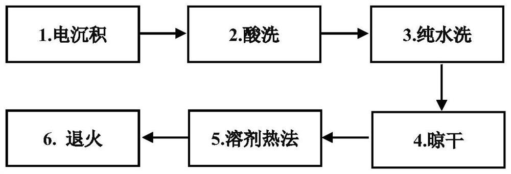
[0041] A preparation of nanostructured WO on the surface of ITO glass 3 Low-energy, high-efficiency methods for thin films, such as figure 1 shown, including the following steps:
[0042] The sample to be processed in this embodiment is a circular ITO glass with a diameter of 37mm and a square resistance of 10Ω.
[0043] A. Preparation of WO on ITO glass by electrodeposition 3 seed layer;
[0044] Prepare 0.1mol / L Na in the electroplating pool 2 WO 4 500mL of aqueous solution, the cleaned sample was used as cathode insertion solution with an area of 54cm 2 The Pt electrode used as the anode is inserted into the solution, the distance between the two electrodes is 2.5cm, the constant current, the current density is 1.25mA / cm 2 , after electrodeposition at room temperature for 200s, it was taken out to obtain a dark brown sample. ...
Embodiment 2
[0049] Example 2: Preparation of seed layer by pulse electrodeposition and then solvothermal growth of nanostructured WO 3 film
[0050] A preparation of nanostructured WO on the surface of ITO glass 3 Low-energy, high-efficiency methods for thin films, such as figure 1 shown, including the following steps:
[0051] The sample to be processed in this embodiment is a circular ITO glass with a diameter of 37mm and a square resistance of 10Ω.
[0052] A. Preparation of WO on ITO glass by electrodeposition 3 seed layer;
[0053] Prepare 0.1mol / L Na 2 WO 4 500mL of aqueous solution, adding H at a concentration of 0.1mol / L 2 SO 4 Make the pH of the electroplating solution = 7, and use the cleaned sample as the cathode insertion solution, with an area of 54 cm 2 The Pt electrode used as the anode is inserted into the solution, the distance between the two electrodes is 2.5cm, using unidirectional pulse electrodeposition, the frequency is 100Hz, the on-off ratio is 1:1, and...
Embodiment 3
[0059] A preparation of nanostructured WO on the surface of ITO glass 3 Low-energy, high-efficiency methods for thin films, such as figure 1 shown, including the following steps:
[0060] The sample to be processed in this embodiment is a circular ITO glass with a diameter of 37mm and a square resistance of 10Ω.
[0061] A. Preparation of WO on ITO glass by electrodeposition 3 seed layer;
[0062] Prepare 0.01mol / L K in the electroplating pool 2 WO 4 500mL of aqueous solution, the cleaned sample was used as the cathode insertion solution, with an area of 53.76cm 2 The graphite electrode used as the anode is inserted into the solution, the distance between the two electrodes is 2.5cm, the constant current, the current density is 0.1mA / cm 2 , taken out after electrodeposition at room temperature for 600s, and the sample was obtained.
[0063] B. Pickling: prepare 500mL of 0.001mol / L hydrochloric acid in the pickling tank, clamp the sample with wooden clamps and rinse it...
PUM
| Property | Measurement | Unit |
|---|---|---|
| concentration | aaaaa | aaaaa |
| diameter | aaaaa | aaaaa |
| electrical resistance | aaaaa | aaaaa |
Abstract
Description
Claims
Application Information
 - R&D
- Intellectual Property
- Life Sciences
- Materials
- Tech Scout
- Unparalleled Data Quality
- Higher Quality Content
- 60% Fewer Hallucinations
Browse by: Latest US Patents, China's latest patents, Technical Efficacy Thesaurus, Application Domain, Technology Topic, Popular Technical Reports.
© 2025 PatSnap. All rights reserved.Legal|Privacy policy|Modern Slavery Act Transparency Statement|Sitemap|About US| Contact US: help@patsnap.com