
Back-electrode-free photoelectric detector array structure adopting TSV technology and preparation method thereof

A photodetector, array structure technology, applied in the direction of electric solid devices, circuits, electrical components, etc., can solve the problems of cost reduction, poor effect, unfavorable device thinning, etc., and achieve the effect of reducing production costs

Inactive Publication Date: 2019-11-29
江苏尚飞光电科技股份有限公司
View PDF0 Cites 0 Cited by
  • Summary
  • Abstract
  • Description
  • Claims
  • Application Information

AI Technical Summary

Problems solved by technology

[0003] At present, mainstream photodetectors adopt a PIN structure with a back electrode, and the anode and cathode of the detector are respectively located on the front and back of the detector, which does not take advantage of device thinning and cost reduction; in addition, in order to reduce the crosstalk of the detector array, usually Using PN junction isolation, deep trench isolation and other technologies, the effect is not good or the process is difficult

Method used


Image

  • Back-electrode-free photoelectric detector array structure adopting TSV technology and preparation method thereof
  • Back-electrode-free photoelectric detector array structure adopting TSV technology and preparation method thereof

Examples


Embodiment Construction

[0018] The present invention is described below in conjunction with accompanying drawing.

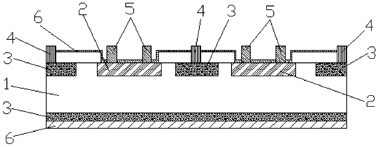
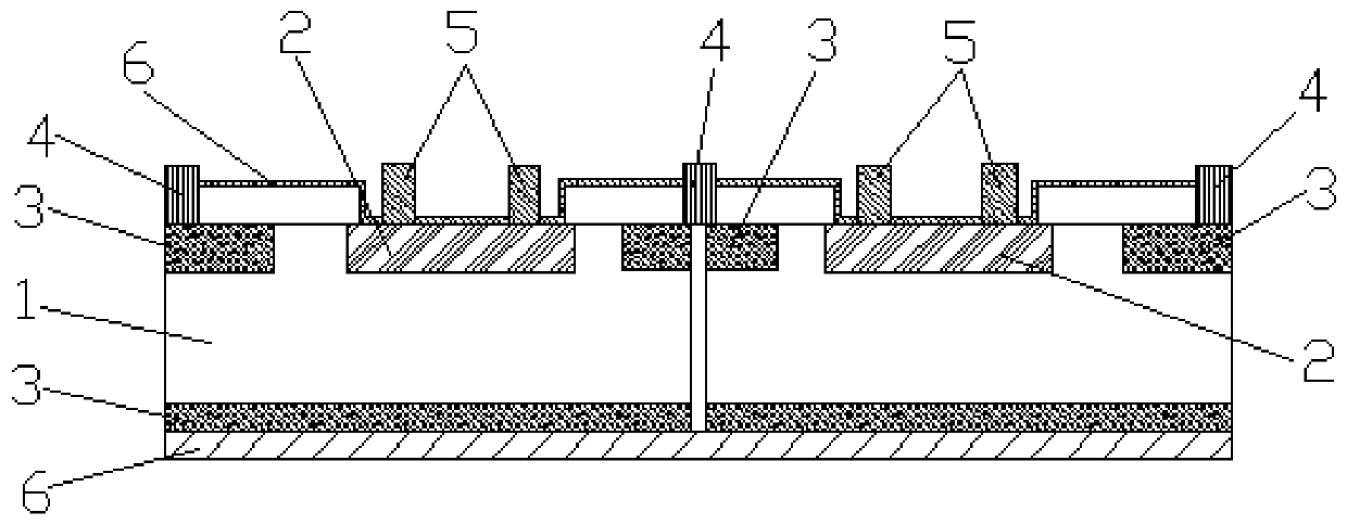
[0019] as attached figure 1 , 2 Shown is a back-electrode-free photodetector array structure using TSV technology according to the present invention, including a semiconductor silicon substrate 1, a P+ type isolation groove 2 and an N+ doped region 3; the P+ type isolation groove 2 is set On the front side of the semiconductor silicon substrate 1; the N+ doped region 3 is arranged on the front side and the back side of the semiconductor silicon substrate 1; the P+ type isolation groove 2 and the N+ doped region 3 on the front side of the semiconductor silicon substrate 1 are alternately spaced Setting; the N+ doped region 3 on the front of the semiconductor silicon substrate 1 is provided with an electrode cathode 4; the upper end of the P+ type isolation groove 2 is provided with an electrode anode 5; the front and back of the semiconductor silicon substrate 1 are also provided with ...


PUM

PropertyMeasurementUnit
Thicknessaaaaaaaaaa

Abstract

The invention discloses a back-electrode-free photoelectric detector array structure adopting a TSV technology and a preparation method thereof. The structure comprises a semiconductor silicon substrate, P+ type isolation grooves and N+ doping regions, wherein the P+ type isolation grooves are arranged in the front surface of the semiconductor silicon substrate; the N+ doping regions are arrangedon the front surface and the back surface of the semiconductor silicon substrate; the P+ type isolation grooves and the N+ doping regions on the front surface of the semiconductor silicon substrate are arranged at intervals in a staggered manner; the N+ doping region on the front surface of the semiconductor silicon substrate is provided with an electrode cathode; the upper end of the P+ type isolation groove is provided with an electrode anode; the front surface and the back surface of the semiconductor silicon substrate are provided with anti-reflecting films; and the electrode cathode and the electrode anode are arranged at the same side. Through arranging the electrodes at the same time, the light and thin development requirement of a detector device is met, the production cost is reduced, the N+ doping regions on the front surface and the back surface of the semiconductor silicon substrate adopt the TSV technology, communication of the N+ doping regions on the front surface and the back surface is realized, and carrier collection and crosstalk reduction are facilitated.

Description

technical field [0001] The invention relates to a back-electrode-free photodetector array structure using TSV technology and a preparation method thereof, belonging to the technical field of semiconductor photodetectors. Background technique [0002] The semiconductor photodetector array generates visible light in the scintillator through direct incident light or X-rays, and generates non-equilibrium carriers in the semiconductor to detect the incident light. The key parameters to measure the performance of the photodetector array include resolution, dark current, Signal-to-noise ratio, readout speed, and charge crosstalk between pixels, etc. [0003] At present, mainstream photodetectors adopt a PIN structure with a back electrode, and the anode and cathode of the detector are respectively located on the front and back of the detector, which does not take advantage of device thinning and cost reduction; in addition, in order to reduce the crosstalk of the detector array, us...

Claims


Application Information

Patent Timeline
IPC IPC(8): H01L27/144H01L31/0216H01L31/0224H01L31/0352H01L31/18
CPCH01L27/1443H01L27/1446H01L31/02161H01L31/022408H01L31/035272H01L31/1804H01L31/1868Y02P70/50
Inventor 董自勇盛振汪斌李文刚
Owner 江苏尚飞光电科技股份有限公司
Learn More