

Silicon carbide semiconductor device terminal and manufacturing method thereof
A semiconductor and silicon carbide technology, which is applied in the field of silicon carbide semiconductor device preparation, can solve the problems of large terminal area, small occupied wafer area, high tolerance of terminal doping concentration, etc., and achieve the effect of high tolerance and small terminal area
- Summary
- Abstract
- Description
- Claims
- Application Information
AI Technical Summary
Problems solved by technology
Method used
Image

Examples
Embodiment Construction
[0035] In order to make the object, technical solution and advantages of the present invention clearer, the present invention will be further described in detail below in conjunction with specific embodiments and with reference to the accompanying drawings.
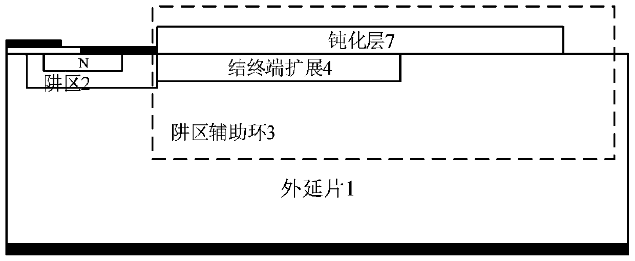
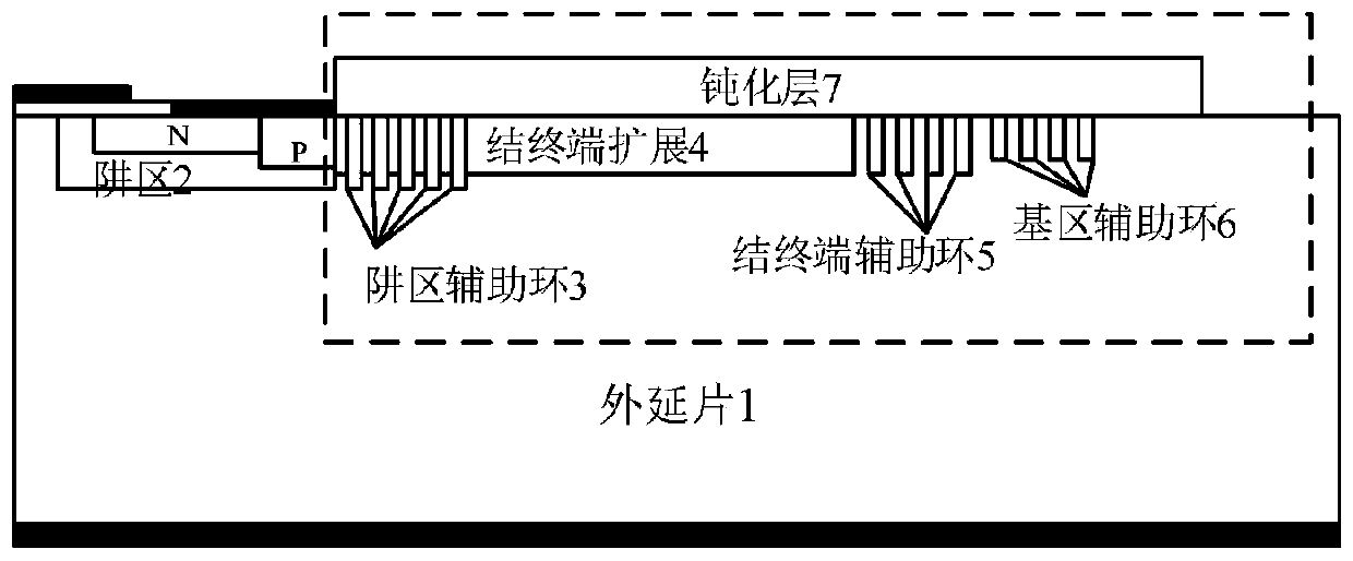
[0036] An aspect of the embodiments of the present invention provides a silicon carbide device terminal structure, figure 1 It is a schematic diagram of the structure of a silicon carbide MOSFET adopting an embodiment of the present invention, wherein the terminal structure of the silicon carbide device proposed by the present invention is inside the dotted line box. Such as figure 1 As shown, the terminal includes several auxiliary rings of the well region (3), a junction terminal extension (4), several auxiliary rings of the junction termination (5), several auxiliary rings of the base region (6) and a passivation layer (7 ). The well region auxiliary ring (3) is located outside the well region (2), and the junction...
PUM
 Abstract
Description
Claims
Application Information