Compound solar cell containing superlattice structure back field
A solar cell and superlattice technology, applied in the field of solar cells, can solve the problems of restricting the performance of solar cells, unable to suppress diffusion, limiting open circuit voltage, etc., to achieve the effect of improving efficiency, improving quality, and reducing the drop of open circuit voltage.
- Summary
- Abstract
- Description
- Claims
- Application Information
AI Technical Summary
Problems solved by technology
Method used
Image
Examples
Embodiment 1
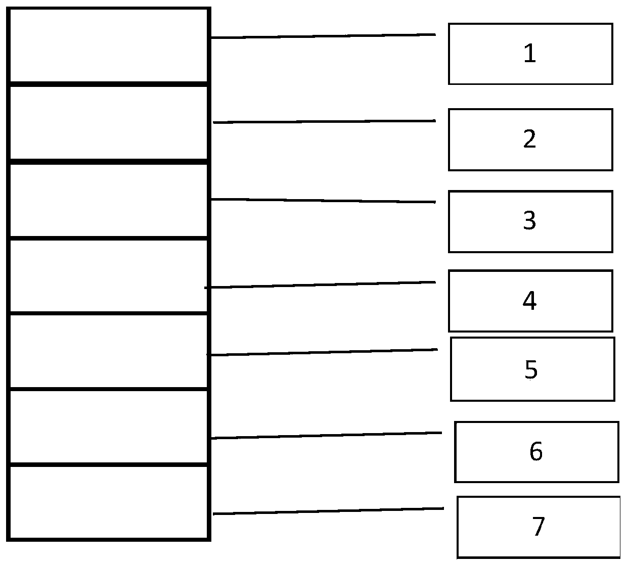
[0041] Take the fourth (0.73eV) solar cell in the four-junction solar cell as an example, such as image 3 As shown, the cell includes an n-type doped n++ layer 1, a highly p-type doped p++ layer 2, a superlattice back field region 3, a p layer 4, an i layer 5, an n layer 6, and a window layer arranged in sequence. 7.
[0042] n++ layer 1, using In 0.47 Ga 0.477 al 0.053 As, the band gap is 0.8eV, the thickness is 15nm, the doping element is Si, and the doping concentration is 5x10 19 cm -3 .
[0043] p++ layer 2, using In 0.47 Ga 0.477 al 0.053 As, the band gap is 0.8eV, the thickness is 15nm, the doping element is Zn, and the doping concentration is 2x10 19 cm -3 .
[0044] The back field region 3 contains 5 pairs of InAlAs / InP superlattice, the thickness of each layer of InAlAs and InP is 2nm, the doping element is Zn, and the doping concentration of InAlAs is 1x10 18 cm -3 , InP doping concentration 5x10 17 cm -3 .
[0045] The thickness of p layer 4 adopts...
Embodiment 2
[0052] Take the fifth (0.88eV) solar cell in the five-junction solar cell as an example, such as image 3 As shown, the cell includes an n-type doped n++ layer 1, a highly p-type doped p++ layer 2, a superlattice back field region 3, a p layer 4, an i layer 5, an n layer 6, and a window layer arranged in sequence. 7.
[0053] n++ layer 1, using In 0.47 Ga 0.424 al 0.106 As, the band gap is 0.9eV, the thickness is 15nm, the doping element is Si, and the doping concentration is 5x10 19 cm -3 .
[0054] p++ layer 2, using In 0.47 Ga 0.424 al 0.106 As, the band gap is 0.9eV, the thickness is 15nm, the doping element is Zn, and the doping concentration is 2x10 19 cm -3 .
[0055] The back field region 3 contains 5 pairs of InAlAs / InP superlattice, the thickness of each layer of InAlAs and InP is 2nm, the doping element is Zn, and the doping concentration of InAlAs is 1x10 18 cm -3 , InP doping concentration 5x10 17 cm -3 .
[0056] The thickness of p layer 4 adopts ...
PUM
| Property | Measurement | Unit |
|---|---|---|
| Thickness | aaaaa | aaaaa |
| Thickness | aaaaa | aaaaa |
| Thickness | aaaaa | aaaaa |
Abstract
Description
Claims
Application Information


