Manufacturing method of externally-convex transparent conductive film

A technology of transparent conductive film and conductive film, which is applied in the direction of printed circuit manufacturing, conductive pattern formation, electrical components, etc., can solve the problems of waste liquid environment impact, complicated manufacturing process, poor conductivity, etc., and achieve improved discoloration efficiency and improved The effect of overall performance and strong electrical conductivity

Inactive Publication Date: 2019-12-03
WUJIANG YOUXIN NEW MATERIAL TECH
View PDF3 Cites 1 Cited by
  • Summary
  • Abstract
  • Description
  • Claims
  • Application Information

AI Technical Summary

Problems solved by technology

[0003] Conventional transparent metal conductive films are mostly realized by printing conductive ink after yellow photolithography or uv transfer printing structure. The cost of the former is high, and its waste liquid has an impact on the environment and wastes a lot. The production process of the latter is complicated and due to the conductive material It is hidden inside the uv structure and cannot be in direct contact with external materials, so the conductivity is relatively poor

Method used


Image

  • Manufacturing method of externally-convex transparent conductive film

Examples


Embodiment Construction

[0028] The following will clearly and completely describe the technical solutions in the embodiments of the present invention with reference to the accompanying drawings in the embodiments of the present invention. Obviously, the described embodiments are only some, not all, embodiments of the present invention. Based on the embodiments of the present invention, all other embodiments obtained by persons of ordinary skill in the art without making creative efforts belong to the protection scope of the present invention.

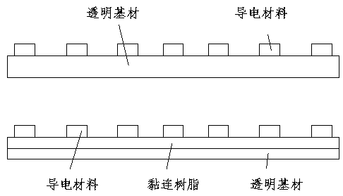
[0029] see figure 1 , the present invention provides a technical solution: a method for preparing a convex transparent conductive film, comprising the following steps:

[0030] ①. Preparation of base material

[0031] The conductive material is directly filled into the groove of the uv structure by micro-nano printing, and then the conductive material inside the groove is transferred to the surface of the transparent substrate to form a transparent conductive...


PUM


Abstract

The invention relates to the micro nano printing technology field and especially relates to a manufacturing method of an externally-convex transparent conductive film. The method comprises the following steps of manufacturing a base material; directly filling a conductive material in a uv structure groove through a micro-nano printing mode; transferring the conductive material in the groove to a surface of a transparent base material to form a transparent conductive film through static electricity and viscosity of a uv glue in an uv transfer printing mode; coating a uv resin, preparing a pet optical bare material or other optical base materials after one embedded transparent conductive film is manufactured; coating the uv resin on the pet optical bare material or the other optical base materials or the embedded conductive film; and laminating the two materials in a same-size ratio manner, and then carrying out roller impressing. In the invention, advantages of a small resistance and strong conductivity are achieved, a conductive layer is directly based on an optical material without interference of other media, simultaneously a phenomenon that a waste liquid in yellow photoetchingpollutes an environment is avoided, pollution to the environment is prevented, production cost is reduced, and losses of a source material are reduced.

Description

technical field [0001] The invention relates to the field of micro-nano printing technology, in particular to a method for preparing a convex transparent conductive film. Background technique [0002] Transparent conductive film is a kind of film that can conduct electricity and has high transparency in the visible light range, mainly including metal film system, oxide film system, other compound film system, polymer film system, composite film system, etc. [0003] Conventional transparent metal conductive films are mostly realized by printing conductive ink after yellow photolithography or uv transfer printing structure. The cost of the former is high, and its waste liquid has an impact on the environment and wastes a lot. The production process of the latter is complicated and due to the conductive material It is hidden inside the uv structure and cannot be in direct contact with external materials, so the conductivity is relatively poor. The present invention further ex...

Claims


Application Information

Patent Timeline
Patent Type & Authority Applications(China)
IPC IPC(8): H05K3/12H05K3/20H05K1/03
CPCH05K1/036H05K3/1275H05K3/20
Inventor 姚艳芳
Owner WUJIANG YOUXIN NEW MATERIAL TECH
Why Eureka
Try Eureka