Supercharge Your Innovation With Domain-Expert AI Agents!

Wafer manufacturing tool and method of use thereof

A wafer and tool technology, applied in the field of wafer manufacturing tools, can solve problems such as reducing finishing processing, and achieve the effects of reducing finishing processing, improving production efficiency, and increasing cutting accuracy

Active Publication Date: 2021-08-06
SHANGLUO UNIV
View PDF0 Cites 0 Cited by
  • Summary
  • Abstract
  • Description
  • Claims
  • Application Information

AI Technical Summary

Problems solved by technology

[0006] Aiming at the problems existing in the prior art, the object of the present invention is to provide a wafer manufacturing tool and its use method, which uses water to cut single crystal silicon rods, and is not prone to high temperature during the cutting process to cause edge chipping, Defects such as microcracks and delamination, and the cutting thickness of silicon wafers is determined by the technicians themselves, instead of only cutting thin wafers. The surface of the cut silicon wafers is relatively flat, which greatly reduces subsequent finishing processing and greatly improves Wafer production rate

Method used


Image

  • Wafer manufacturing tool and method of use thereof
  • Wafer manufacturing tool and method of use thereof
  • Wafer manufacturing tool and method of use thereof

Examples


Embodiment 1

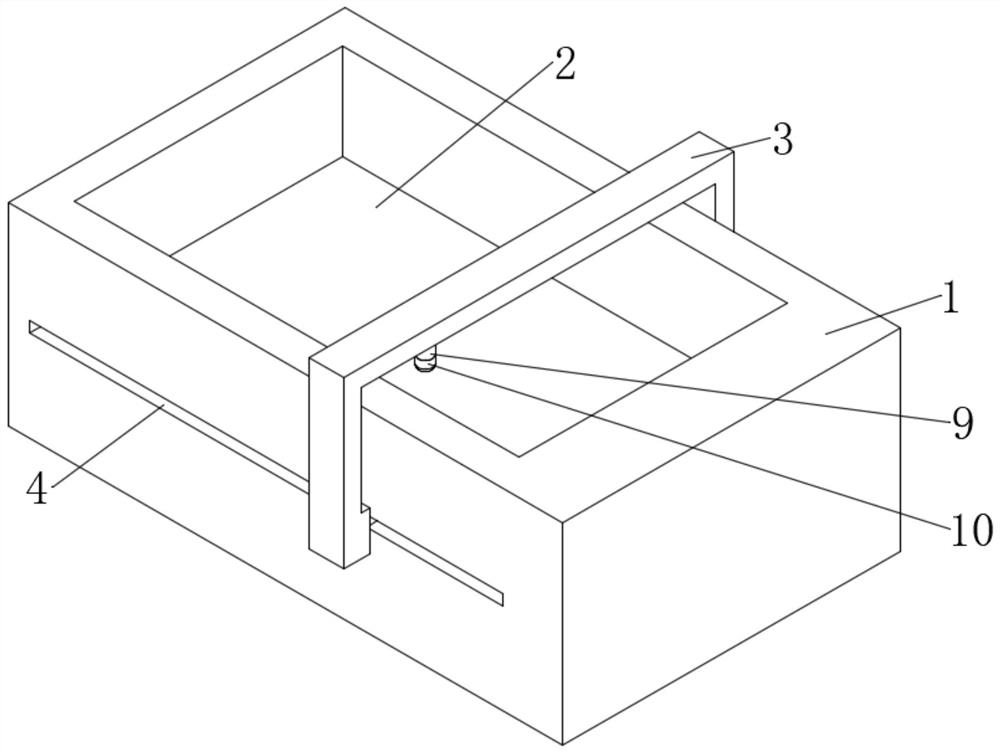
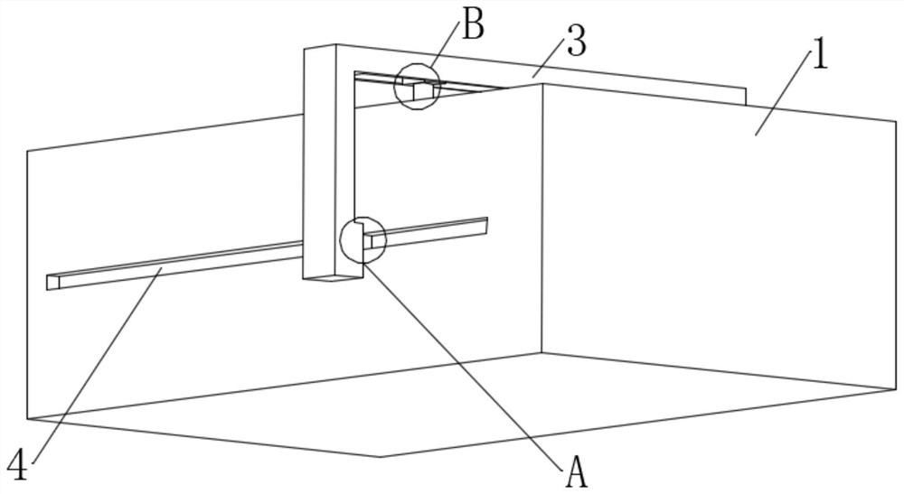
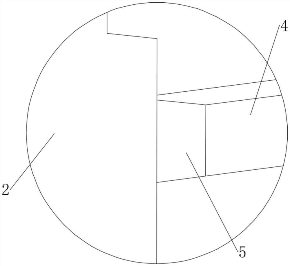
[0043] see Figure 1-6 , a wafer manufacturing tool, comprising a base 1, the upper end of the base 1 is dug with a water tank 2, the upper side of the base 1 is provided with a main body 3 of a mechanical arm, and the main body 3 of the mechanical arm is in the shape of a "door". A pair of first electromagnetic slide rails 4 are excavated on the side wall of the table 1, and the ends of the lower ends of the two mechanical arm bodies 3 close to the base 1 are fixedly connected with the first electromagnetic slide blocks 5 matching the first electromagnetic slide rails 4, The base 1 and the main body of the mechanical arm 3 are slidably connected through the first electromagnetic slide rail 4 and the first electromagnetic slider 5. A second electromagnetic slide rail 7 is excavated on the side close to the base 1 at the upper end of the main body 3 of the mechanical arm. The second electromagnetic slide rail 7 is slidably connected with a second electromagnetic slider 8, and o...


PUM


Abstract

The invention discloses a wafer manufacturing tool and a method for using the same, belonging to the field of wafer manufacturing, a wafer manufacturing tool and a method for using the same. The invention realizes the cutting of single crystal silicon rods by using water cutting technology, water cutting The surface of the prepared silicon wafer is smooth, and it is not easy to have defects such as chipping, micro-cracks and delamination. At the same time, the water jet used for cutting does not have the problem of loss, and it is not easy to cause thermal burst due to overheating of the cutting tool itself, and it is not easy to affect the cutting quality. , the water jet itself will also cool the silicon rods, so that the silicon rods are not easily deformed in a small amount under high-temperature cutting conditions, and it is not easy to affect the product accuracy of the silicon wafers produced by cutting, which greatly reduces the precision of the silicon wafers before photolithography. Processing, and in the process of water cutting, the cutting positioning automation is realized through the control terminal, without manual operation by technicians, which greatly increases the cutting accuracy, improves the production efficiency of the wafer, and increases the quality of the wafer.

Description

technical field [0001] The present invention relates to the field of wafer manufacturing, more specifically, to a wafer manufacturing tool and a method for using the same. Background technique [0002] Wafer refers to the silicon wafer used in the production of silicon semiconductor integrated circuits. Because of its circular shape, it is called a wafer. It can be processed into various circuit element structures on the silicon wafer and become an IC with specific electrical functions. product. [0003] In the process of wafer preparation, single crystal silicon rods are usually prepared first, and then the single crystal silicon rods are cut and finished, and finally photolithography is carried out. Among them, the silicon wafer cutting methods mainly include diamond grinding wheel cutting, laser cutting : Laser cutting uses the high temperature generated by the high-energy laser beam to instantly gasify the silicon material in the irradiated local area and complete the s...

Claims


Application Information

Patent Timeline
Patent Type & Authority Patents(China)
IPC IPC(8): B24C1/04B24C3/02B24C5/04B24C9/00
CPCB24C1/045B24C3/02B24C5/04B24C9/00
Inventor 唐卫斌王博何建强鱼轮
Owner SHANGLUO UNIV
Features
  • R&D
  • Intellectual Property
  • Life Sciences
  • Materials
  • Tech Scout
  • Unparalleled Data Quality
  • Higher Quality Content
  • 60% Fewer Hallucinations
Learn More