Gold nanometer wafer

A nano-chip and gold technology, applied in the direction of hypodermic injection devices, needles, and devices introduced into the body, can solve the problems of inconspicuous use, low safety, and insufficient sharpness, and achieve rapid onset of effect, improved absorption, and enhanced The effect of using the effect

Pending Publication Date: 2019-12-20
丁丽丽
View PDF0 Cites 1 Cited by
  • Summary
  • Abstract
  • Description
  • Claims
  • Application Information

AI Technical Summary

Problems solved by technology

[0002] Nanochip is a special tool for nano-penetration enhancement developed according to the structure of human skin. It is carved from single crystal silicon through nanotechnology. The surface of nanochip is a series of microneedle arrays, which can open the outermost stratum corneum of the skin. At the same time, it will not hurt the dermis, greatly improving the penetrat

Method used


Image

  • Gold nanometer wafer
  • Gold nanometer wafer
  • Gold nanometer wafer

Examples


Embodiment Construction

[0016] The following will clearly and completely describe the technical solutions in the embodiments of the present invention with reference to the accompanying drawings in the embodiments of the present invention. Obviously, the described embodiments are only some, not all, embodiments of the present invention.

[0017] In describing the present invention, it should be understood that the terms "upper", "lower", "front", "rear", "left", "right", "top", "bottom", "inner", " The orientation or positional relationship indicated by "outside", etc. is based on the orientation or positional relationship shown in the drawings, and is only for the convenience of describing the present invention and simplifying the description, rather than indicating or implying that the referred device or element must have a specific orientation, so as to Specific orientation configurations and operations, therefore, are not to be construed as limitations on the invention.

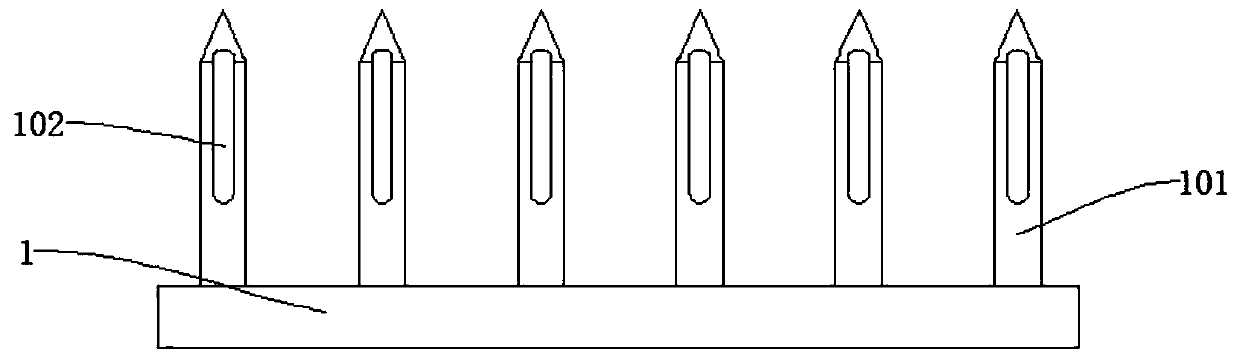
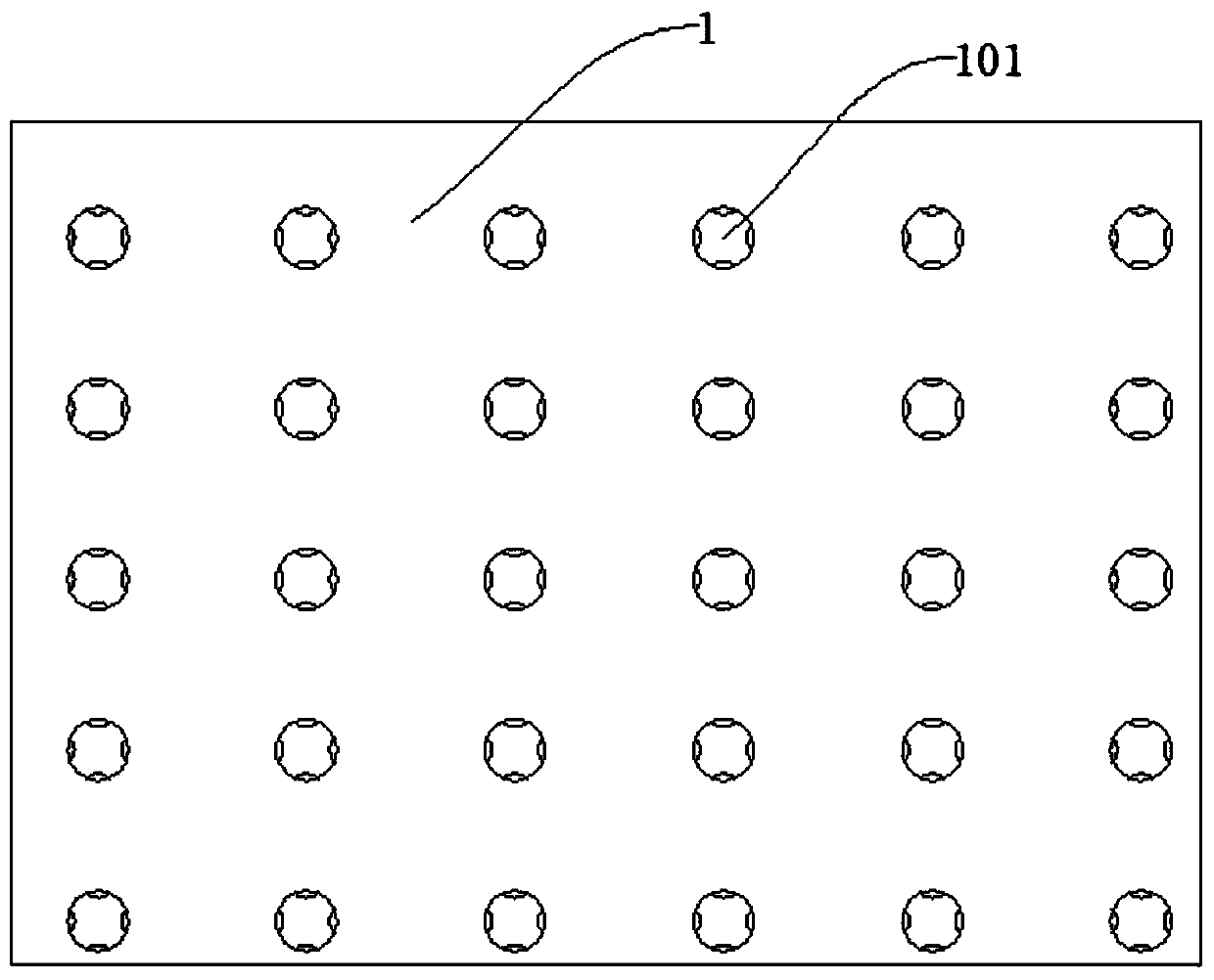
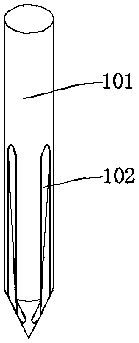
[0018] refer to Figure ...


PUM


Abstract

The invention discloses a gold nanometer wafer, and belongs to the technical field of a nanometer wafer. The gold nanometer wafer comprises a silicon substrate, wherein microneedles are arranged on the silicon substrate; each microneedle comprises an upper section and a lower section; the upper section of the microneedle is in a cylindrical shape; the lower section of the microneedle is in a pointed cone shape; a groove is formed in each microneedle; and a gold layer is plated on the outer wall of each microneedle. The gold nanometer wafer has the advantages that by using an independent research and development technology, 99.999-percent gold materials are combined with 99.999-percent monocrystalline silicon materials; through a fine engraving process, the nanometer level microneedles areintegrated onto the wafer; the use effect is obvious; and effective active substances can be conveyed to positions above the stratum basale, so that the seepage of a skin care product is greatly enhanced, and the skin care product fast works; and the corium layer, nerves and blood vessels cannot be touched, so that no harm is caused on the skin.

Description

technical field [0001] The invention relates to the technical field of nano-chips, in particular to a gold nano-chip. Background technique [0002] Nanochip is a special tool for nano-penetration enhancement developed according to the structure of human skin. It is carved from single crystal silicon through nanotechnology. The surface of nanochip is a series of microneedle arrays, which can open the outermost stratum corneum of the skin. At the same time, it will not hurt the dermis, greatly improving the penetration of nutrients, and the biocompatibility of monocrystalline silicon ensures the safety of nanocrystals during use. However, the current nanochips are less safe in use and will affect people Causes a certain degree of pain, takes effect slowly, and the effect of use is not obvious, and most of the microneedles used have the disadvantages of not being sharp enough at the tip and easy to break. Contents of the invention [0003] The purpose of the present inventio...

Claims


Application Information

Patent Timeline
IPC IPC(8): A61M37/00
CPCA61M37/0015A61M2037/0007A61M2037/0023
Inventor 丁丽丽
Owner 丁丽丽
Why Eureka
Try Eureka