
Method and system for repairing time sequence violations in chip design

A chip design and timing technology, applied in computing, special data processing applications, instruments, etc., can solve the problems of not being able to guarantee complete timing analysis, lack of control of results, and failure to meet design requirements, so as to save design time, Reduce design cost and save area

Active Publication Date: 2019-12-20
MOLCHIP TECH (SHANGHAI) CO LTD
View PDF6 Cites 21 Cited by
  • Summary
  • Abstract
  • Description
  • Claims
  • Application Information

AI Technical Summary

Problems solved by technology

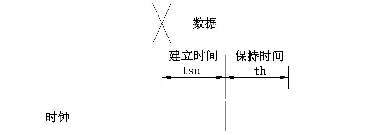
[0005] 1) If additional protection time is added to the timing path that has already met the design requirements, layout and wiring will result in the addition of a large number of redundant basic units in the timing path, increasing the area of ​​the chip and increasing the design cost
[0006] 2) For the timing path that does not meet the design requirements, if additional guard time is added to place and route again, because the tools used in the placement and routing stage and the timing analysis stage are different, it may also occur that a certain timing path meets the requirements in the placement and routing tool. The design requirements but the timing analysis tool analyzes the problem that does not meet the design requirements, and repeated iterations of the same method will waste a lot of time
It not only lengthens the design cycle, but also cannot guarantee that the next layout and routing results will fully meet the timing analysis, which is a waste of time and lacks control over the results

Method used


Image

  • Method and system for repairing time sequence violations in chip design
  • Method and system for repairing time sequence violations in chip design
  • Method and system for repairing time sequence violations in chip design

Examples


Embodiment

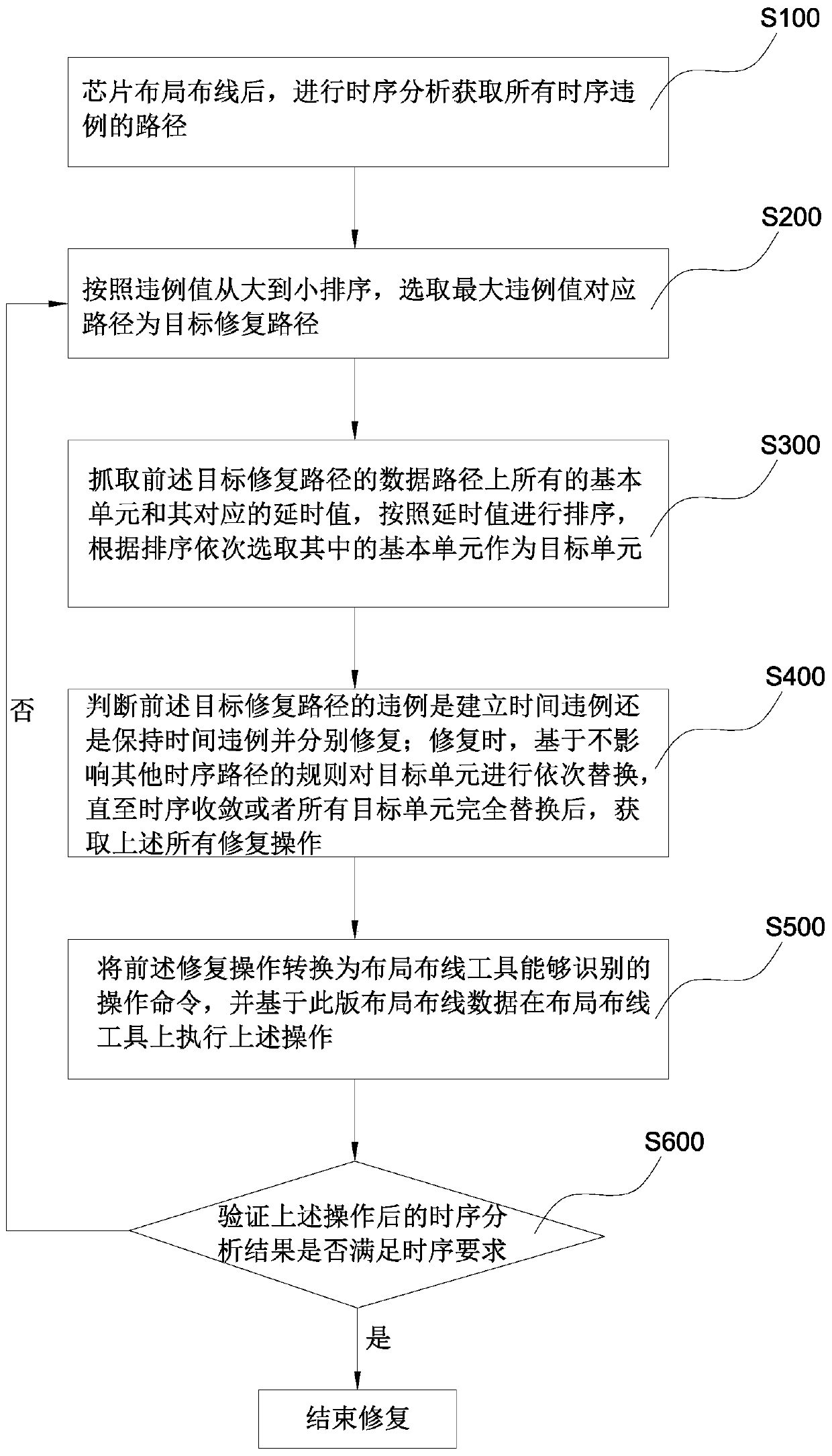
[0066] see figure 2 As shown, a method for repairing timing violations in chip design is provided, including the following steps:

[0067] Step 100, after the chip layout and routing, perform timing analysis based on timing analysis tools to obtain all timing violation paths.

[0068] After completing the chip layout and routing, extract the netlist information and SPEF (Standard Parasitic Parameter Exchange Format) information of the chip layout and routing, perform timing analysis based on the preset timing constraints under the timing analysis tool, and list according to the results of the aforementioned timing analysis Paths for all timing violations.

[0069] The preset timing constraint condition, as an example rather than limitation, may come from a timing constraint file in a design specification, for example.

[0070] Step 200, sort the violation values ​​in descending order, and select the path corresponding to the largest violation value as the target repair path...


PUM


Abstract

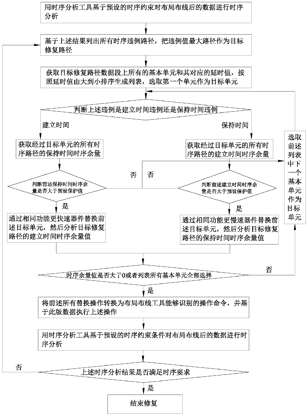
The invention discloses a method and system for repairing time sequence violations in chip design, and relates to the technical field of integrated circuit design. The method comprises the following steps of selecting a target repair path from time sequence violation paths, grabbing all basic units and the delay values corresponding to the basic units in the target repair path and sorting, and sequentially selecting the basic units as the target units according to the sequence; judging whether the violation is an establishment time violation or a retention time violation, replacing the targetunits sequentially based on the rules which do not affect other time sequence paths, and obtaining the repair operation meeting requirements; and converting the repair operation into an operation command which can be identified by a layout wiring tool, executing the operation on the layout wiring tool, and ending the repair under the condition of verifying that the time sequence analysis result after the operation meets the time sequence requirement. According to the invention, when the time sequence violation repair is carried out, the re-layout and the re-wiring are not needed, and the timesequence convergence can be realized through the rapid iteration.

Description

technical field [0001] The invention relates to the technical field of integrated circuit design, in particular to a method for repairing timing violations in chip design. Background technique [0002] In the design of integrated circuit chips, the main factors that determine the operating speed and design area of ​​integrated circuit chips are as follows: production process, code writing style, physical implementation process from code to layout, etc. Fixing timing is one of the most important critical steps in the code-to-layout physical implementation process. With the development of deep sub-meter technology, the design process of the chip is getting smaller and smaller, the delay of the connection between the device and the device is becoming more and more unstable, the scale of the chip design is getting bigger and bigger, and the design frequency is getting higher and higher. . Various factors lead to increasingly difficult chip timing convergence. The timing conve...

Claims


Application Information

Patent Timeline
IPC IPC(8): G06F17/50
Inventor 吴帅帅郑立青
Owner MOLCHIP TECH (SHANGHAI) CO LTD
Learn More