flip method

A technology of flip chip and solder column, which is applied in the direction of semiconductor/solid-state device parts, semiconductor devices, electrical components, etc., to avoid collapse and avoid short circuit

Active Publication Date: 2022-01-25
NANTONG FUJITSU MICROELECTRONICS
View PDF8 Cites 0 Cited by
  • Summary
  • Abstract
  • Description
  • Claims
  • Application Information

AI Technical Summary

Problems solved by technology

[0003] However, in the existing flip-chip method, adjacent solder layers are easily connected together

Method used


Image

  • flip method
  • flip method
  • flip method

Examples


Embodiment Construction

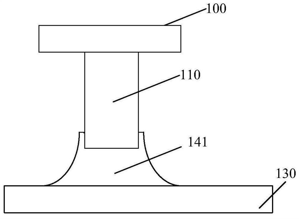
[0019] As mentioned in the background, the flip-chip method formed in the prior art will result in poor quality of the solder layer, and adjacent solder layers are easily connected together.

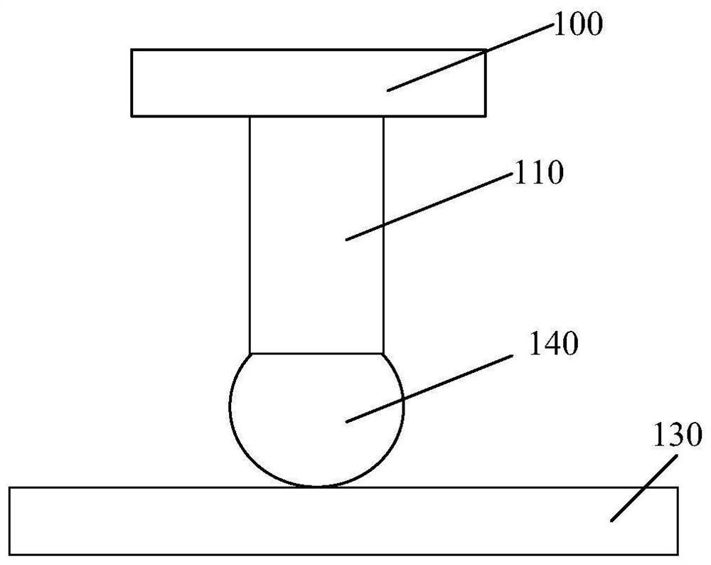
[0020] Figure 1 to Figure 2 is a schematic diagram of the structure of the flip-chip method.

[0021] refer to figure 1 , providing a semiconductor chip 100, a conductive connecting column 110 and a carrier plate 130, the conductive connecting column 110 has an opposite first surface and a second surface; the conductive connecting column 110 is fixed on the surface of the semiconductor chip 100, the first Facing the semiconductor chip 100; the solder ball 140 is fixedly arranged on the second surface of the conductive connection column 110; after that, the semiconductor chip 100, the conductive connection column 110 and the solder ball 140 are placed on the surface of the carrier board 130, and the solder ball 140 is connected to the surface of the carrier plate 130. The carrier board...


PUM

PropertyMeasurementUnit
thicknessaaaaaaaaaa
thicknessaaaaaaaaaa

Abstract

A flip-chip method, comprising: providing a semiconductor chip and a conductive connection post, the conductive connection post having opposite first surfaces and a second surface; fixing the conductive connection post on the surface of the semiconductor chip, with the first surface facing the semiconductor chip; a carrier board is provided; solder pillars are formed on the surface of the carrier board; a barrier layer is formed, the barrier layer is located on the surface of the carrier board around the solder pillars; after the barrier layer is formed, the solder pillars and The second surface is in contact, and the conductive connection post is located on the solder post; after the solder post is brought into contact with the second surface, reflow soldering is performed, and the solder post forms a solder layer. The method avoids connecting adjacent solder layers together.

Description

technical field [0001] The invention relates to the packaging field, in particular to a flip-chip method. Background technique [0002] The flip chip process is not only a chip interconnection technology, but also an ideal chip bonding technology. As early as more than 50 years ago, IBM (International Business Machines Corporation) has developed and used this technology. But until recent years, flip-chip has become a frequently used package formation in the field of high-end devices and high-density packaging. At present, the application range of flip-chip packaging technology is becoming wider and wider, and the packaging forms are becoming more diversified, and the requirements for flip-chips are also increasing. [0003] However, in the existing flip-chip method, adjacent solder layers are easily connected together. Contents of the invention [0004] The problem solved by the present invention is to provide a flip-chip method which avoids connecting adjacent solder l...

Claims


Application Information

Patent Timeline
Patent Type & Authority Patents(China)
IPC IPC(8): H01L23/49H01L21/48
CPCH01L23/49H01L21/4885H01L2924/181H01L2224/16225H01L2924/00012
Inventor 石磊
Owner NANTONG FUJITSU MICROELECTRONICS
Why Eureka
Try Eureka