Schottky diode and preparation method thereof
A Schottky diode and Schottky metal technology, which is applied in semiconductor/solid-state device manufacturing, semiconductor devices, electrical components, etc., can solve problems such as difficulty in obtaining Schottky barrier height and single characteristics
- Summary
- Abstract
- Description
- Claims
- Application Information
AI Technical Summary
Problems solved by technology
Method used
Image

Examples
specific Embodiment approach 1
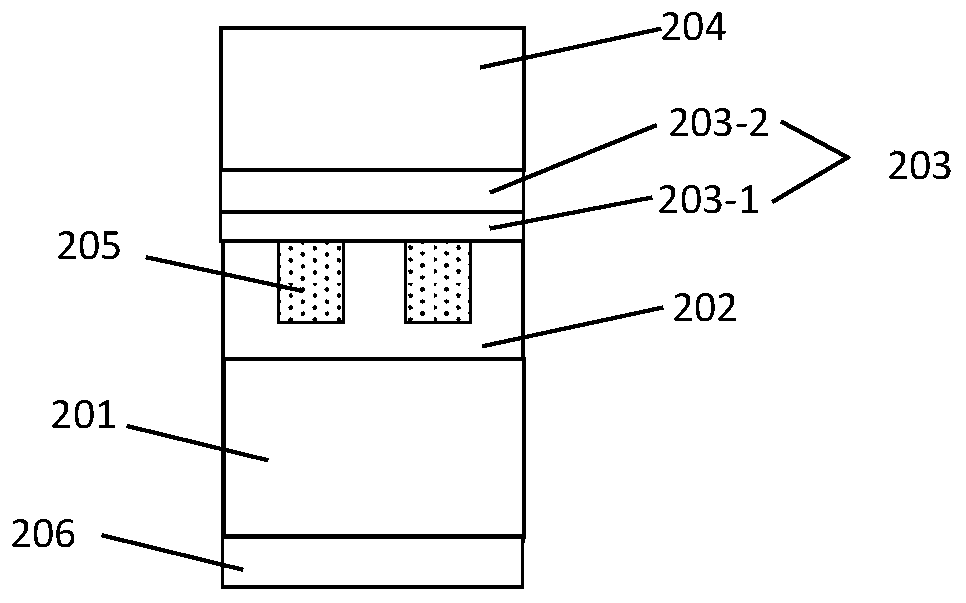
[0024] Such as figure 2 As shown in , the Schottky diode of the present invention includes an N+ substrate 201, an N- epitaxial layer 202, p+ implantation regions 205 arranged at equal intervals in the N-epitaxial layer 202, and a Schottky metal unit 203 (including the first Schottky metal layer 203 - 1 and second Schottky metal layer 203 - 2 ), anode metal 204 and cathode metal 206 . The first Schottky metal 203-1 is in direct contact with the upper surface of the silicon carbide epitaxial layer 202 and the p+ implantation region 205, the second Schottky metal 203-2 is directly deposited on the surface of the first Schottky metal 203-1, After the deposition of 203-1 and 203-2 is completed, rapid annealing is performed at the same time, the temperature range is 400-600°C, and the time is 5 minutes. After the annealing is completed, the first Schottky metal 203-1 (such as Al metal) and the second Schottky metal 203-2 (such as Mo metal) undergo an alloying reaction with silico...
specific Embodiment approach 2
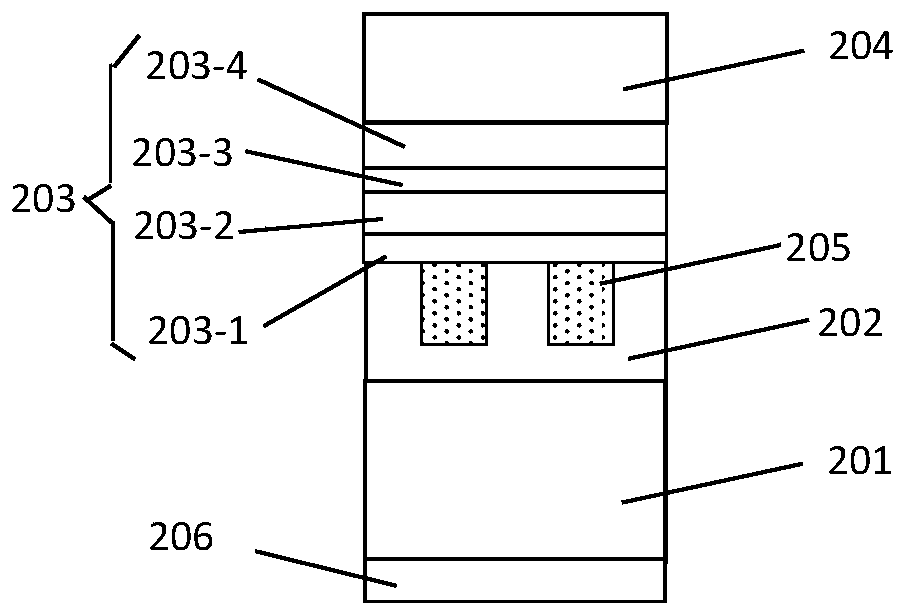
[0030] Such as image 3 As shown, on the basis of Embodiment 1, a third metal layer 203-3 and a fourth metal layer 203-4 are added;
[0031] Wherein, the N- epitaxial layer 202 includes at least two layers of Schottky contact metals with different work functions, and the first metal layer 203-1 directly in contact with the silicon carbide epitaxial layer is a metal with a low work function. It is the second metal layer 203-2 whose work function is higher than that of the first metal layer 203-1, wherein the odd-numbered layers are metals with the same type of low work function as the first metal layer 203-1, such as Al, Ti, etc., and the even-numbered layers are It is the same kind of high work function metal as the second metal layer 203-2, such as Mo, Au and the like. No matter how many layers of metal the Schottky metal is composed of, its total thickness remains constant at a specific value, preferably 200 nm. All the metal layers above form Schottky junctions with the s...
specific Embodiment approach 3
[0034] The preparation method of Schottky diode of the present invention specifically comprises the following steps:
[0035] Step 1, forming an N- epitaxial layer 202 on the N+ substrate 201;
[0036] Step 2, making a p+ implantation region 205 on the N- epitaxial layer 202;
[0037] Step 3. Deposit the first metal layer in the Schottky metal unit 203 to the N- epitaxial layer 202 by sputtering, and then deposit the second metal layer on the first metal layer, and so on, to complete the deposition , and then form a Schottky junction by annealing, the Schottky metal layer unit 203 includes multiple layers of Schottky metal layers (203-1, 203-2, 203-3, 203-4), and two adjacent The metal work functions of the Schottky metal layers are different;
[0038] Step 4. Precipitating cathode metal 206 and anode metal 204 .
PUM
| Property | Measurement | Unit |
|---|---|---|
| Thickness | aaaaa | aaaaa |
Abstract
Description
Claims
Application Information
 - R&D
- Intellectual Property
- Life Sciences
- Materials
- Tech Scout
- Unparalleled Data Quality
- Higher Quality Content
- 60% Fewer Hallucinations
Browse by: Latest US Patents, China's latest patents, Technical Efficacy Thesaurus, Application Domain, Technology Topic, Popular Technical Reports.
© 2025 PatSnap. All rights reserved.Legal|Privacy policy|Modern Slavery Act Transparency Statement|Sitemap|About US| Contact US: help@patsnap.com