
Micro-nano-scale speckle manufacturing method

A manufacturing method and micro-nano-scale technology, which are applied in the photoengraving process, instruments, optics and other directions of the pattern surface, can solve the problems of small manufacturing area, complex technical problems and high cost, and achieve high size and density accuracy and simple process. Flexible, low-cost effects

Inactive Publication Date: 2019-12-27
WUHAN UNIV
View PDF11 Cites 1 Cited by
  • Summary
  • Abstract
  • Description
  • Claims
  • Application Information

AI Technical Summary

Problems solved by technology

[0003] At present, the commonly used speckle production methods are artificial speckle production methods, such as using a roller to produce speckle spots. The speckle particles produced by this method are relatively large, and the shape and size of the speckle produced often cannot reach the actual optimal size. When the surface of the test piece has many textures, bumps, indentations and bumps, it is often troublesome to use the roller to make it
In addition, there are chemical vapor deposition methods and ultraviolet lithography methods to make micro-nano scale speckles. These two methods are too complicated to make speckles, and the speckle particles are difficult to control, and the production area is small and the cost is high.
[0004] The traditional way of making speckles is to use ultraviolet exposure lithography to create speckles, but ultraviolet exposure lithography faces expensive lithography equipment and complex technical problems, such as avoiding optical diffraction and lens material selection, etc.

Method used


Image

  • Micro-nano-scale speckle manufacturing method
  • Micro-nano-scale speckle manufacturing method
  • Micro-nano-scale speckle manufacturing method

Examples


specific Embodiment

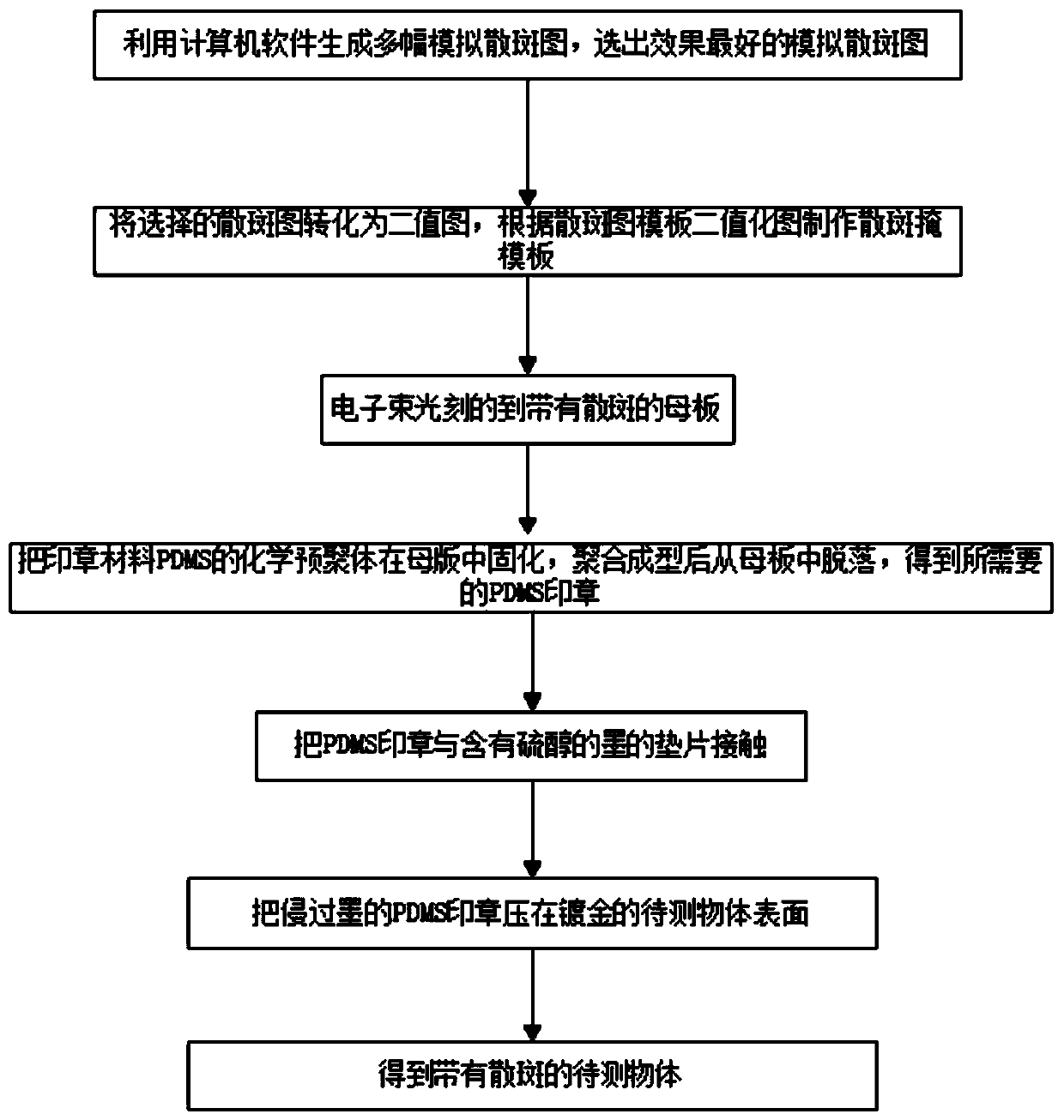
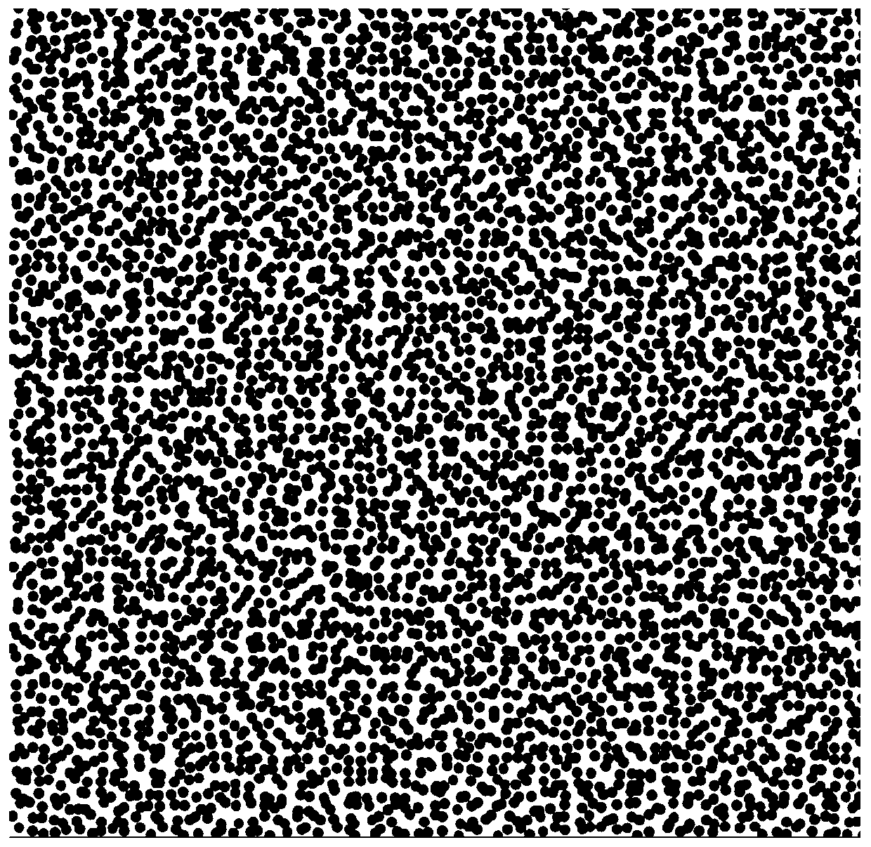
[0024] Using computer software to generate multiple simulated speckle images with different speckle sizes and numbers, the Gaussian algorithm is used in this embodiment, and the gray levels of each speckle can be expressed by the following function:

[0025]

[0026] Among them, s is the number of speckle particles; R is the size of speckle particles; two-dimensional random variable (x k ,y k ) is the center position of the kth speckle particle; I K is the gray value of the center of the kth speckle particle.

[0027] Select the best simulation image according to the average gray gradient sum of the image, and convert the speckle image into a binary image, where the average gray gradient square sum of the image can be expressed by the following function:

[0028]

[0029] M and N are the height and width of the image respectively, in pixels, is the modulus of the gray gradient vector of each pixel. A laser printer will be used to print the binary speckle pattern ont...


PUM


Abstract

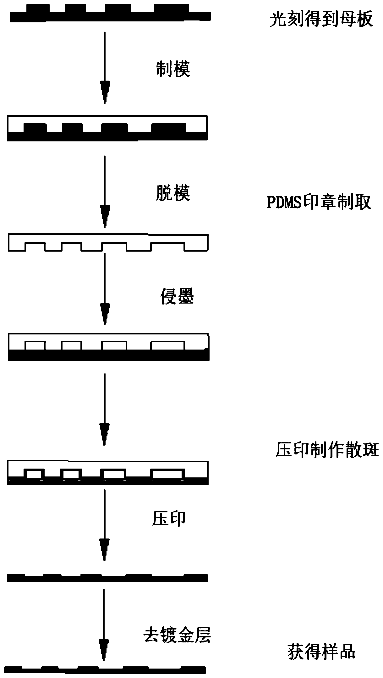
The invention designs a micro-nano-scale speckle manufacturing method. The method comprises the steps of generating multiple simulated speckle patterns with different particle sizes and numbers by using computer software, selecting an optimal simulated speckle pattern from the simulated speckle patterns, converting the speckle pattern into a binary pattern, and printing the speckle binary patternon a plastic polymer sheet to be used as a mask; and then obtaining a mother board with speckles through etching, curing the chemical prepolymer of the seal material PDMS in the mother board, droppingoff the chemical prepolymer from the mother board after polymerization molding to obtain a PDMS seal, enabling the PDMS seal to contact a gasket containing ink, and pressing the PDMS seal which has been soaked in the ink on a surface of the gold-plated to-be-detected object to obtain the to-be-detected object with the speckles. The method disclosed by the invention has the advantages of being simple and quick in manufacturing, convenient to operate, low in cost and efficient in batch.

Description

technical field [0001] The invention belongs to the technical field of photomechanical speckle production, and in particular relates to a micro-nano-scale speckle production method. Background technique [0002] Digital Image Correlation (i.e.DIC) measurement technology is an image measurement method using computer vision technology, and it is a non-contact method for full-field shape, deformation, and motion measurement. It is the product of the combination of modern advanced photoelectric technology, image processing and recognition technology and computer technology, and it is another new progress in the field of modern light side mechanics. It uses randomly distributed spots on the surface of objects or pseudo-randomly distributed artificial speckle fields as deformation information carriers, and is a new experimental mechanical method for full-field displacement and strain analysis of materials or structural surfaces under the action of external loads or other factors. ...

Claims


Application Information

Patent Timeline
IPC IPC(8): G02B27/48G03F7/00
CPCG02B27/48G03F7/0002
Inventor 陈志文刘胜马坤杨凡王晨阳
Owner WUHAN UNIV
Learn More