Back contact heterojunction solar cell and manufacturing method thereof

A technology of solar cells and heterojunctions, applied in the direction of final product manufacturing, sustainable manufacturing/processing, circuits, etc., can solve the problems of cumbersome manufacturing process, narrow material selection range, easy short circuit, etc., to increase the process window, improve the Efficiency, the effect of improving short-circuit current

Inactive Publication Date: 2019-12-31
GOLD STONE (FUJIAN) ENERGY CO LTD
View PDF9 Cites 1 Cited by
  • Summary
  • Abstract
  • Description
  • Claims
  • Application Information

AI Technical Summary

Problems solved by technology

[0003] However, the P-type semiconductors and N-type semiconductors formed on the back of the battery with this structure exist alternately, and short circuits are prone to occur between them.
In order to effectively isolate P-type semiconductors and N-type semiconductors, multiple protection and etching processes are required. The manufacturing process is cumbersome and easily affects the quality of the amorphous silicon film layer, making it difficult to achieve high conversion efficiency.
Especially due to the difficult etching of the P-type amorphous silicon layer, the selection range of materials is very narrow, such as the etching selectivity cannot meet the requirements, and the device cannot work normally.

Method used


Image

  • Back contact heterojunction solar cell and manufacturing method thereof
  • Back contact heterojunction solar cell and manufacturing method thereof
  • Back contact heterojunction solar cell and manufacturing method thereof

Examples


Embodiment

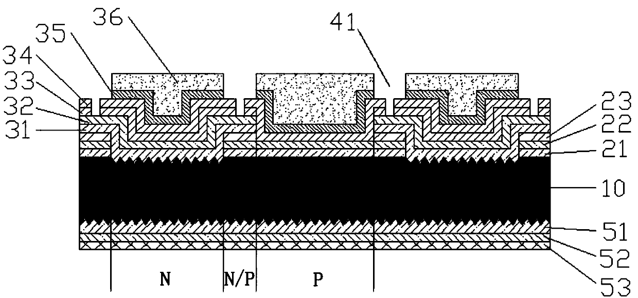
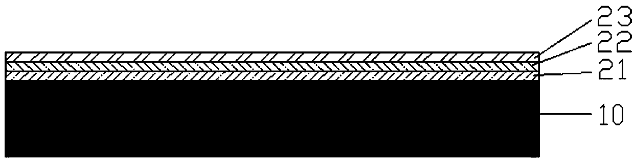
[0037] refer to figure 1 , a back-contact heterojunction solar cell, comprising an N-type monocrystalline silicon wafer 10, a second intrinsic amorphous silicon layer 51 and a first N-type amorphous silicon layer successively arranged on the pyramidal textured surface of the front surface of the silicon wafer 10 52. A layer of anti-reflection layer 53, which is sequentially arranged on the first intrinsic amorphous silicon layer 21, the P-type amorphous silicon layer 22, the second transparent conductive film layer 34, and the copper seed layer 35 on the surface of the P region on the back of the silicon wafer 10. , copper grid line electrode 36, the third intrinsic amorphous silicon layer 31, the second N-type amorphous silicon layer 32, the first transparent conductive film layer 33, the first transparent conductive film layer 33, the third intrinsic amorphous silicon layer 31, the second N-type amorphous silicon layer, etc. Two transparent conductive film layers 34, a coppe...


PUM

PropertyMeasurementUnit
Thicknessaaaaaaaaaa
Thicknessaaaaaaaaaa
Widthaaaaaaaaaa

Abstract

The invention discloses a back contact heterojunction solar cell and a manufacturing method thereof. The cell comprises an N-type monocrystalline silicon wafer, a second intrinsic amorphous silicon layer, a first N-type amorphous silicon layer and an anti-reflection layer sequentially arranged on the pyramidal texture on the front of the silicon wafer, a first intrinsic amorphous silicon layer, aP-type amorphous silicon layer, a second transparent conductive film layer, a copper seed layer and a copper grid line electrode sequentially arranged in a P region on the back surface of the siliconwafer, a third intrinsic amorphous silicon layer, a second N-type amorphous silicon layer, a first transparent conductive film layer, a second transparent conductive film layer, a copper seed layer and a copper grid line electrode sequentially arranged on the N-region pyramidal texture of the back surface of the silicon wafer, and a first intrinsic amorphous silicon layer, a P-type amorphous silicon layer, an insulating layer, a third intrinsic amorphous silicon layer, a second N-type amorphous silicon layer, a first transparent conductive film layer, a second transparent conductive film layer, a copper seed layer and an insulating groove sequentially arranged on the surface of an N / P overlapping region on the back surface of the silicon wafer. The method can greatly increase process windows, is more suitable for large-scale mass production, improves the short circuit current and open circuit voltage of a cell, and improves the efficiency of a cell piece.

Description

technical field [0001] The invention relates to the field of crystalline silicon solar cells, in particular to a back contact heterojunction solar cell and a manufacturing method thereof. Background technique [0002] Under the energy crisis, the photovoltaic industry is developing rapidly. The key to further promoting photovoltaic applications is to improve the photoelectric conversion efficiency of solar cells and reduce the production cost of cells. Back-contact heterojunction solar cells are a good combination of back-contact structure cells and silicon-based heterojunction cells. The back contact structure is by concentrating the electrodes on the back of the solar cell. Since there is no shading of the front grid electrode, the cell has a high short-circuit current; the silicon-based heterojunction cell can be relieved due to the high-quality hydrogenated amorphous silicon passivation The holes and electrons generated under the light recombine and disappear inside the...

Claims


Application Information

Patent Timeline
IPC IPC(8): H01L31/0236H01L31/075H01L31/20
CPCH01L31/02363H01L31/075H01L31/202Y02E10/548Y02P70/50
Inventor 曾清华张超华谢志刚王树林林朝晖
Owner GOLD STONE (FUJIAN) ENERGY CO LTD
Why Eureka
Try Eureka