Niobium-based Josephson junction etching method

A technology of junction etching and ion beam etching machine, which is applied in the manufacture/processing of superconductor devices, superconducting devices, electrical components, etc., and can solve problems such as differences in etching methods, impact on device performance, and multi-metal deposition. Achieve the effects of improving yield and productivity, reducing Nb layer damage, and simple etching method

Pending Publication Date: 2019-12-31
JIANGSU LEUVEN INSTR CO LTD
View PDF5 Cites 5 Cited by
  • Summary
  • Abstract
  • Description
  • Claims
  • Application Information

AI Technical Summary

Problems solved by technology

In the case of severe deposition, in addition to organic deposition, there are more metal depositions, which are difficult to clean and have a significant impact on device performance
[0006] like image 3 , during the Josephson junction etch, the Nb layer and the AlO x The properties of the / Al layer are different, and the etching method is also different. If etching with chlorine-based gas, AlO x / Al layer is easy to absorb chloride ions and cause corrosion

Method used


Image

  • Niobium-based Josephson junction etching method
  • Niobium-based Josephson junction etching method
  • Niobium-based Josephson junction etching method

Examples


Embodiment 1

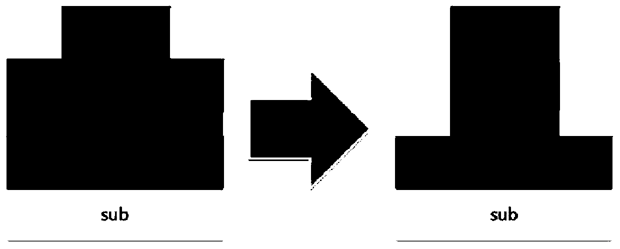
[0037] A niobium-based Josephson junction etching method, see image 3 , the niobium-based Josephson junction includes mask material (Mask), Nb layer, AlO x / Al layer, Nb layer and bottom layer material (sub), the mask material is photoresist, the bottom layer material is Si not as a functional layer, wherein the thickness of the upper Nb layer is 150nm, AlO x The thickness of AlOx in the / Al layer is 1nm, the thickness of the Al layer is 9nm, the thickness of the lower Nb layer is 150nm, and the shape of the device is a truncated cone. The etching gas is C4F8; the inert gas is Ar gas.

[0038] The niobium-based Josephson junction is under the condition of not interrupting the vacuum environment during processing, and the specific steps of the etching method are as follows:

[0039] Step 1. In a vacuum state, put the niobium-based Josephson junction sample to be etched into the transfer device, and the transfer device transfers the sample to the reactive ion etching chamber;...

Embodiment 2

[0045] A niobium-based Josephson junction etching method, the niobium-based Josephson junction sequentially includes mask material (Mask), Nb layer, AlO x / Al layer, Nb layer and bottom layer material (sub), the mask material is a hard mask, and the bottom layer material is SiO, which is not used as a functional layer. The thickness of the upper Nb layer is 150nm, AlO x The thickness of AlOx in the / Al layer is 1nm, the thickness of the Al layer is 9nm, the thickness of the lower Nb layer is 150nm, and the shape of the device is square platform. The etching gas is C4F8, and the etching gas is He.

[0046] The niobium-based Josephson junction is under the condition of not interrupting the vacuum environment during processing, and the specific steps of the etching method are as follows:

[0047] Step 1. In a vacuum state, put the niobium-based Josephson junction sample to be etched into the transfer device, and the transfer device transfers the sample to the reactive ion etchi...

Embodiment 3

[0053] A niobium-based Josephson junction etching method, the niobium-based Josephson junction sequentially includes mask material (Mask), Nb layer, AlO x / Al layer, Nb layer and bottom layer material (sub), the mask material is photoresist, and the bottom layer material is SiN, which is not used as a functional layer. The thickness of the upper Nb layer is 150nm, AlO x The thickness of AlOx in the / Al layer is 1nm, the thickness of the Al layer is 9nm, the thickness of the lower Nb layer is 150nm, and the shape of the device is long strip. The etching gas is C4F8, and the inert gas is Ne gas.

[0054] The niobium-based Josephson junction is under the condition of not interrupting the vacuum environment during processing, and the specific steps of the etching method are as follows:

[0055] Step 1. In a vacuum state, put the niobium-based Josephson junction sample to be etched into the transfer device, and the transfer device transfers the sample to the reactive ion etching ...


PUM


Abstract

The invention relates to a niobium-based Josephson junction etching method, and belongs to the technical field of superconducting device preparation. The specific method is as follows: the sample to be etched is sent to a reactive ion etching cavity through a conveying device in the vacuum state, etching gas is introduced and the Nb layer of the sample to be etched is etched; then the sample afterreactive ion etching is sent to an ion beam etching machine through the conveying device in the vacuum state, inert gas is introduced and the AlOx / Al layer is etched; and the Nb-based superconductingdevice is obtained by vacuum extrusion of the sample. The etching method is simple and good in effect, the prepared superconducting device has high yield and productivity, and the device has organicmatter or metal deposition.

Description

technical field [0001] The invention belongs to the technical field of superconducting device preparation, and in particular relates to a niobium-based Josephson junction etching method. Background technique [0002] The phenomenon of superconductivity has been known to the world as early as 1911. At present, various research and development of superconducting technology in my country have been on the right track, and have entered industrial operation, and are now widely used in the power industry, communication field, military field, and medical field. With the development of superconducting technology, the importance of superconducting quantum devices has gradually become prominent, especially in the fields of weak magnetic detection and quantum computing. In superconducting electronic devices, the preparation of Josephson junction is a crucial step. Superconducting materials exhibit zero resistance only at certain temperatures. Superconducting materials are mainly di...

Claims


Application Information

Patent Timeline
Patent Type & Authority Applications(China)
IPC IPC(8): H01L39/24
CPCH10N60/0156H10N60/0884H10N60/0912
Inventor 谷志强吴志浩吴愧蒋中原车东晨许开东
Owner JIANGSU LEUVEN INSTR CO LTD
Why Eureka
Try Eureka