Optical device
An optical device and visible light technology, which is applied in the field of infrared optics, can solve the problem that the optical power of white light is difficult to achieve controllable adjustment, and achieve the effects of adjustable and controllable optical power, good application prospects, and strong anti-interference ability
- Summary
- Abstract
- Description
- Claims
- Application Information
AI Technical Summary
Problems solved by technology
Method used
Image

Examples
Embodiment 1
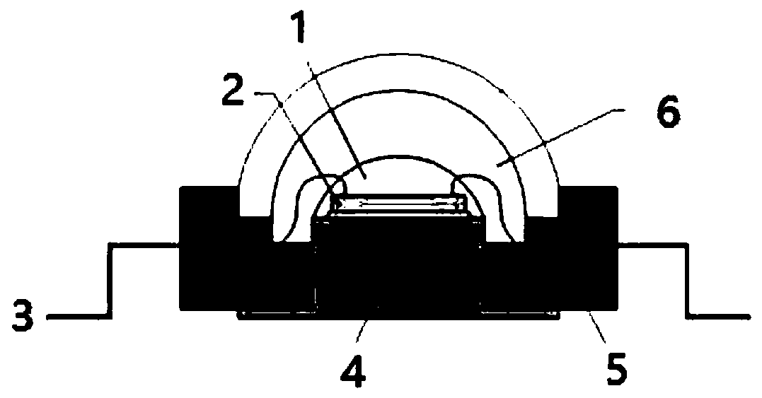
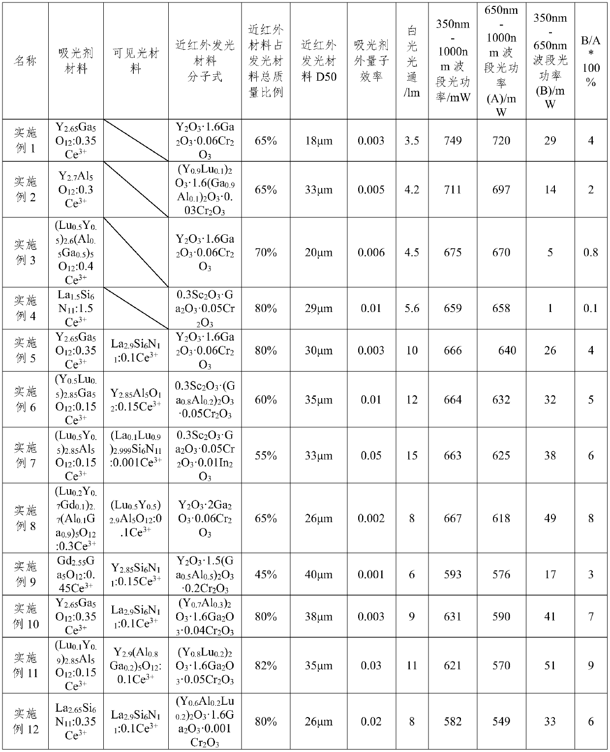
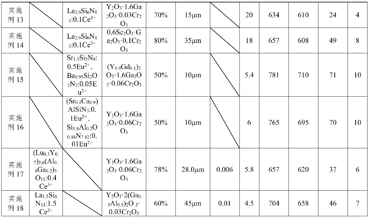
[0041] An optical device, the components of which are blue LED chips with a wavelength of 440nm and a molecular formula of Y 2.65 Ga 5 o 12 :0.35Ce 3+ The light absorber material, the molecular formula is Y 2 o 3 1.6Ga 2 o 3 0.06Cr 2 o 3 The near-infrared luminescent material; wherein the D50 particle size of the near-infrared luminescent material is 18 μm, and the near-infrared luminescent material accounts for 65% of the total mass ratio of the total luminescent material; the external quantum efficiency of the light absorber material is 0.003. Mix the near-infrared luminescent material of the present invention with the resin evenly, stir and defoam to obtain a near-infrared fluorescent conversion layer mixture, cover the mixture on the surface of the LED chip by spraying, and cure it into a near-infrared layer by baking. Fluorescent layer. Then, the light absorbing agent material is mixed with silica gel and evenly coated on the near-infrared fluorescence conversion...
Embodiment 5
[0044] An optical device, the components of which are blue LED chips with a wavelength of 455nm and a molecular formula of Y 2.65 Ga 5 o 12 :0.35Ce 3+ The light absorber material, the molecular formula is La 2.9 Si 6 N 11 :0.1Ce 3+ Visible light material, the molecular formula is Y 2 o 3 1.6Ga 2 o 3 0.06Cr 2 o 3 The near-infrared luminescent material; wherein the D50 particle size of the near-infrared luminescent material is 30 μm, and the near-infrared luminescent material accounts for 80% of the total mass ratio of the total luminescent material; the external quantum efficiency of the light absorber material is 0.003. Mix the near-infrared luminescent material of the present invention with silica gel evenly, stir and defoam to obtain a near-infrared fluorescent conversion layer mixture, cover the mixture on the surface of the LED chip by dispensing, and cure it by baking. Then mix the light absorbing agent material with silica gel and evenly coat it on the near-i...
Embodiment 10
[0047] An optical device, the components of which are blue LED chips with a wavelength of 420nm and a molecular formula of Y 2.65 Ga 5 o 12 :0.35Ce 3+ The light absorber material, the molecular formula is La 2.9 Si6 N 11 :0.1Ce 3+ Visible light material, the molecular formula is (Y 0.7 Al 0.3 ) 2 o 3 1.6Ga 2 o 3 0.04Cr 2 o 3 The near-infrared luminescent material; wherein the D50 particle size of the near-infrared luminescent material is 38 μm, and the near-infrared luminescent material accounts for 80% of the total mass ratio of the total luminescent material; the external quantum efficiency of the light absorber material is 0.003. Mix the near-infrared luminescent material of the present invention with silica gel evenly, stir and defoam to obtain a near-infrared fluorescent conversion layer mixture, cover the mixture on the surface of the LED chip by dispensing, and cure it by baking. Then, the visible light luminescent material and the light absorbing agent mat...
PUM
| Property | Measurement | Unit |
|---|---|---|
| Particle size | aaaaa | aaaaa |
| Particle size | aaaaa | aaaaa |
| Particle size | aaaaa | aaaaa |
Abstract
Description
Claims
Application Information
 - Generate Ideas
- Intellectual Property
- Life Sciences
- Materials
- Tech Scout
- Unparalleled Data Quality
- Higher Quality Content
- 60% Fewer Hallucinations
Browse by: Latest US Patents, China's latest patents, Technical Efficacy Thesaurus, Application Domain, Technology Topic, Popular Technical Reports.
© 2025 PatSnap. All rights reserved.Legal|Privacy policy|Modern Slavery Act Transparency Statement|Sitemap|About US| Contact US: help@patsnap.com