
A detection device and detection method for quickly detecting and identifying surface defects of an optical element

A technology of optical components and identification devices, applied in the field of defect detection, can solve problems such as the inability to quickly detect the surface of large-diameter components, the inability to distinguish defect types, and provide guidance

Active Publication Date: 2020-01-14
SHANGHAI INST OF OPTICS & FINE MECHANICS CHINESE ACAD OF SCI
View PDF4 Cites 5 Cited by
  • Summary
  • Abstract
  • Description
  • Claims
  • Application Information

AI Technical Summary

Problems solved by technology

However, the photothermal weak absorption tester has a very slow measurement speed and cannot be applied to the rapid detection of surface defects of large-diameter components.
Moreover, this method cannot distinguish defect categories, and cannot analyze the source of defects, resulting in the inability to provide guidance for process improvement

Method used


Image

  • A detection device and detection method for quickly detecting and identifying surface defects of an optical element
  • A detection device and detection method for quickly detecting and identifying surface defects of an optical element
  • A detection device and detection method for quickly detecting and identifying surface defects of an optical element

Examples


Embodiment

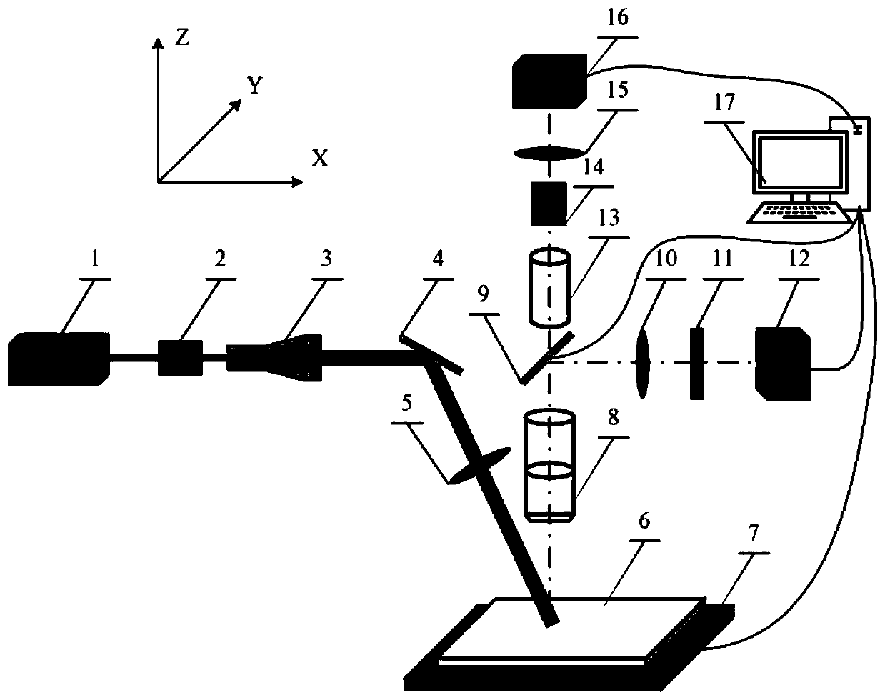
[0027] figure 1 It is a schematic diagram of the rapid detection and identification device for surface defects of optical components of the present invention. It can be seen from the figure that the rapid detection and recognition device of optical components surface defects of the present invention includes a laser 1, a beam shaper 2, a beam expander 3, a mirror 4, and a converging lens 5. Sample 6, XY precision displacement platform 7, zoom lens 8, electric optical path switcher 9, first imaging lens 10, long-wave pass filter 11, first area array photodetector 12, collimator 13, Tuning filter 14, second imaging lens 15, second area array photodetector 16 and computer 17;

[0028] The sample 6 is placed on the XY precision displacement platform 7, and the electric optical path switcher 9 is composed of a reflector installed on an electric flip mount, and the reflective surface of the reflector is perpendicular to the xz plane, The electric flip mounting base can rotate the r...


PUM


Abstract

The invention discloses a detection device and detection method for quickly detecting and identifying surface defects of an optical element. The device mainly comprises a laser, a light beam shaper, abeam expander, a reflector, a convergent lens, a sample, an XY precision displacement platform, a zoom lens, an electric light path switcher, a first imaging lens, a long-wave-pass filter, a first area array photoelectric detector, a collimator, a tunable filter, a second imaging lens, a second area array photoelectric detector and a computer. Defects are imaged by utilizing photoluminescence characteristics of the defects, and rapid detection is realized; and in combination with the hyperspectral imaging technology, the device and method can identify various defects according to the peak characteristics of the luminescence spectrum of the defects, and judge the types of the defects. The detection device designed by the invention integrates rapid detection and identification, and is verysuitable for detection of surface defects of large-aperture optical elements.

Description

technical field [0001] The invention relates to the field of defect detection, in particular to a detection device and a detection method for rapid detection and identification of surface defects of optical elements. Background technique [0002] The laser-induced damage problem of optical components used in large-scale high-power laser devices seriously restricts the improvement of system output flux. The damage of optical components is mainly caused by various defects introduced during the growth stage of optical materials and processing processes such as grinding and polishing. Metal ions Fe introduced during crystal growth 3+ 、Al 3+ 、Cr 3+ , Sb 3+ , Ca 2+ , Pb 2+ 、Si 4+ The light-absorbing centers formed by other impurities lead to the disorder of the local lattice, resulting in the generation of impurity levels in the band gap. During the polishing process of neodymium glass, fused silica glass and other components, the polishing liquid remains on the surface of...

Claims


Application Information

Patent Timeline
Patent Type & Authority Applications(China)
IPC IPC(8): G01N21/63G01N21/01
CPCG01N21/63G01N21/01G01N2021/0112
Inventor 邵建达倪开灶刘世杰周游王圣浩徐天柱潘靖宇白云波
Owner SHANGHAI INST OF OPTICS & FINE MECHANICS CHINESE ACAD OF SCI
Features
  • Generate Ideas
  • Intellectual Property
  • Life Sciences
  • Materials
  • Tech Scout
  • Unparalleled Data Quality
  • Higher Quality Content
  • 60% Fewer Hallucinations
Learn More