
Low-voltage crystal oscillator circuit compatible with GPIO

A crystal oscillator and circuit technology, applied in power oscillators, electrical components, output stability, etc., can solve problems such as failure to meet CMOSIIH leakage current specifications and insufficient isolation

Active Publication Date: 2020-01-17
MICROCHIP TECH INC
View PDF3 Cites 0 Cited by
  • Summary
  • Abstract
  • Description
  • Claims
  • Application Information

AI Technical Summary

Problems solved by technology

However, when the GPIO pads associated with the crystal oscillator circuit are in "external clock" mode and driven by CMOS logic, or in other uses of these GPIO pads, using native NMOS transistor switches will not be sufficient to isolate the oscillation Gm drives the transistor to prevent excessive current leakage through the
Therefore, the CMOS IIH leakage current specification cannot be met

Method used


Image

  • Low-voltage crystal oscillator circuit compatible with GPIO
  • Low-voltage crystal oscillator circuit compatible with GPIO
  • Low-voltage crystal oscillator circuit compatible with GPIO

Examples


Embodiment Construction

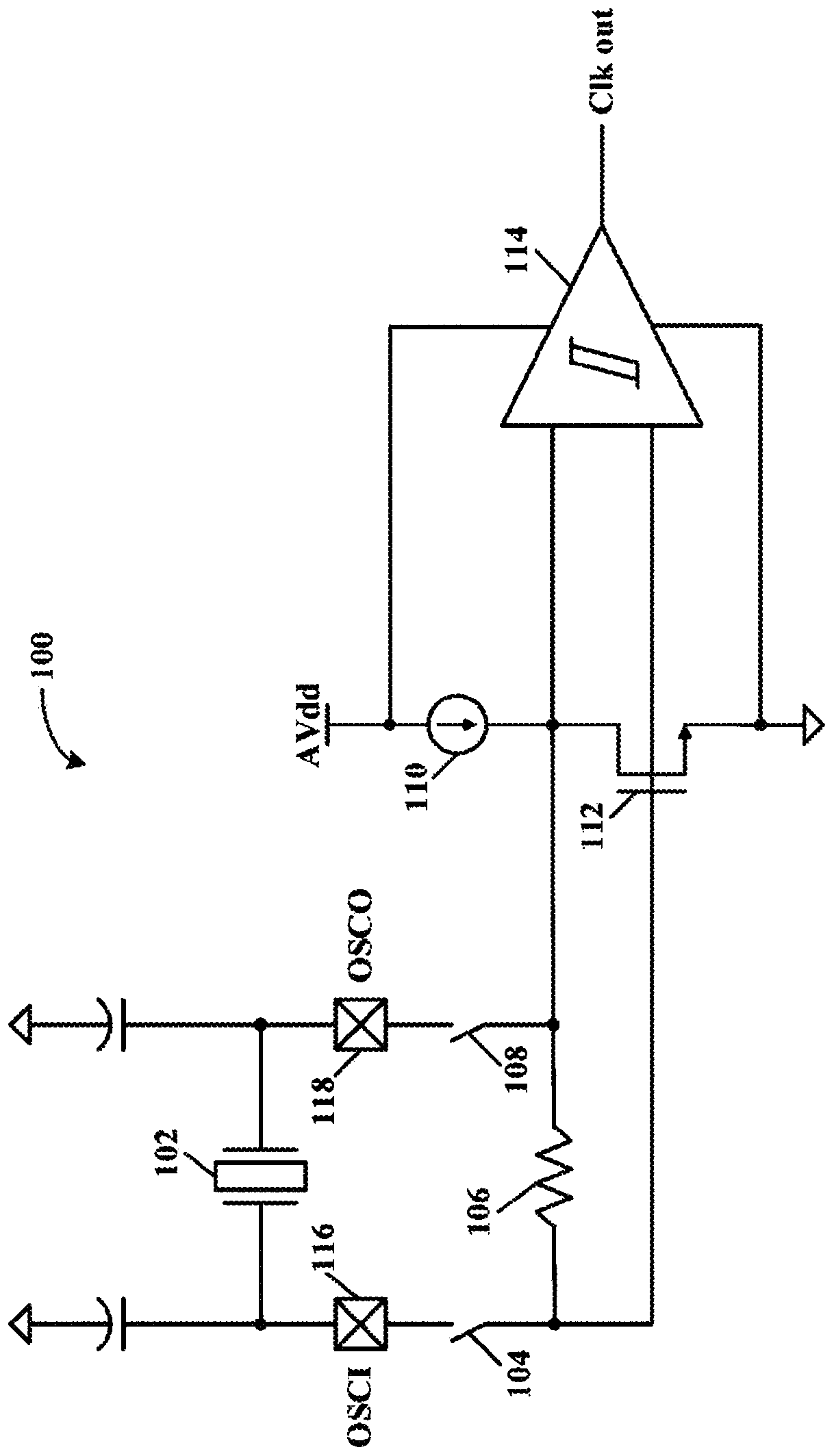
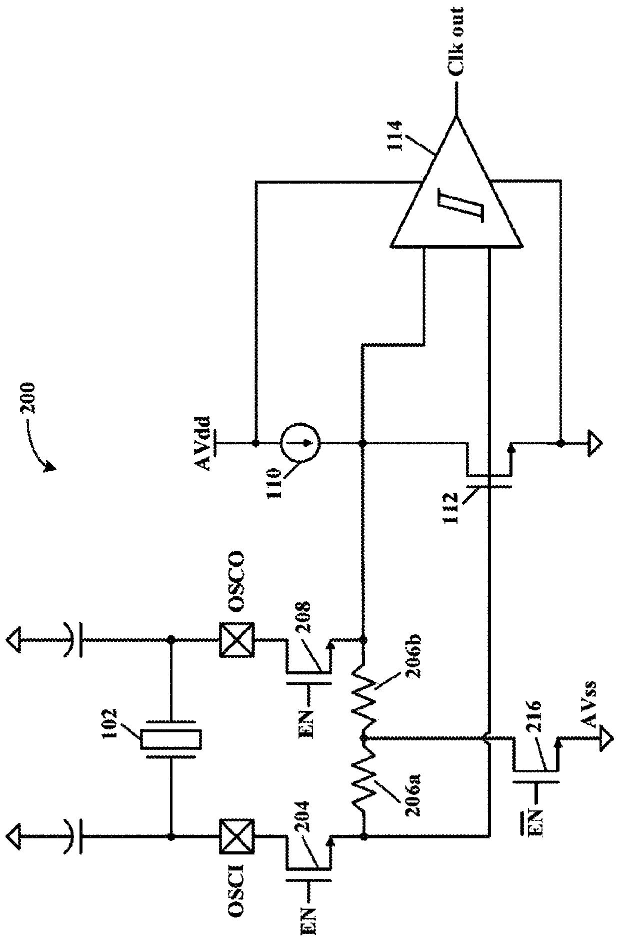
[0019] Various embodiments of the present disclosure can be configured to enable crystal oscillator functionality at a supply voltage (Vdd) that is less than a field effect transistor (FET) threshold (2-Vt). The FET threshold (2-Vt) may be the minimum gate-source voltage required to create a low resistance path between the source and drain of the FET. In some implementations, the crystal oscillator function can be enabled at Vdd less than the FET threshold. In another embodiment, the crystal oscillator function can be enabled at Vdd less than the FET threshold while maintaining the shared GPIO feature. Vdd and AVdd (analog Vdd) will be used interchangeably herein. The Gm (transconductance) of a Metal Oxide Semiconductor Field Effect Transistor (MOSFET) is the change in drain current divided by the smaller change in gate / source voltage, where the drain / source voltage is constant.

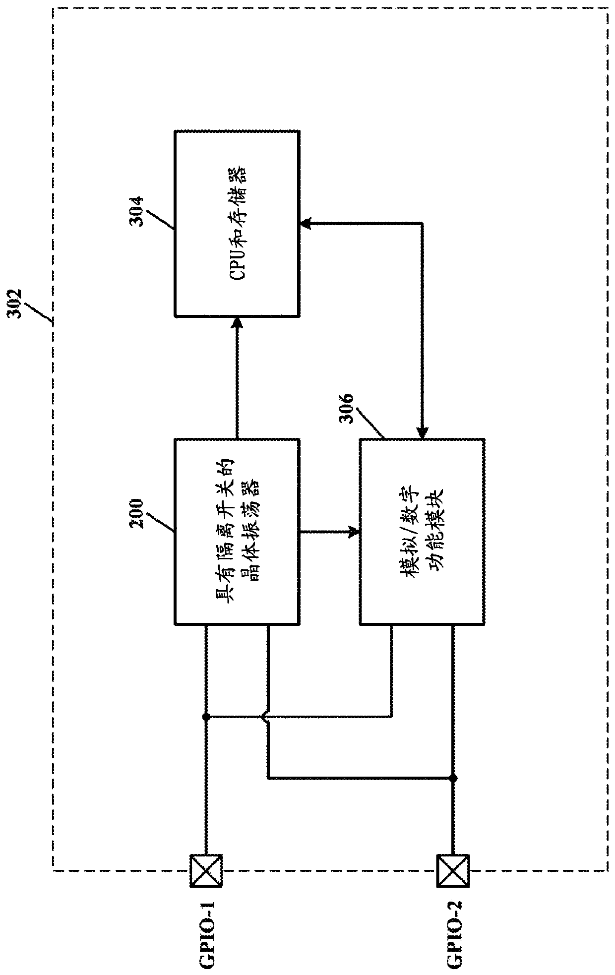
[0020] Referring now to the drawings, details of example embodiments are schematically shown. ...


PUM


Abstract

Low voltage crystal oscillator having native NMOS transistors used for coupling / decoupling to / from GPIO. The native NMOS transistors function properly at a low supply voltage when on (low resistance)and a high supply voltage when off (high resistance). Oscillator Gm driver bias resistors are repurposed to degenerate the native NMOS transistors when they are off, thereby reducing the leakage current thereof (oscillator circuit decoupled from GPIO nodes). This ensures compliance with the CMOS IIH leakage current specification during an external clock (EC) mode at a high supply voltage.

Description

[0001] Related Patent Applications [0002] This application claims priority to commonly-owned US Provisional Patent Application No. 62 / 542,050, filed August 7, 2017; which Provisional Patent Application is hereby incorporated by reference herein for all purposes. technical field [0003] The present disclosure relates to oscillators, and in particular to low voltage crystal oscillator circuits that comply with Complementary Metal Oxide Semiconductor (CMOS) Input Leakage High (IIH) specifications for shared general purpose input output (GPIO) nodes. Background technique [0004] Operation of a low voltage crystal oscillator circuit coupled to a general purpose input output (GPIO) node, such as a connection pad of an integrated circuit (IC), is a desired feature in today's integrated circuit products. However, the low voltage operation of crystal oscillator circuits based on N-channel metal oxide semiconductor (NMOS) Gm drives is limited by the minimum Vdd (supply voltage ) ...

Claims


Application Information

Patent Timeline
Patent Type & Authority Applications(China)
IPC IPC(8): H03B5/36
CPCH03B5/362H03B2200/0082H03B5/364H03B2200/0012H03D2200/009H03B2200/0094H03B5/06H03L1/028
Inventor R·瓦加亚拉加万A·库玛K·卡尔尼克
Owner MICROCHIP TECH INC
Learn More