Method for improving optical switching frequency of GaN ultraviolet detector

A technology of ultraviolet detector and optical switch, which is applied in the field of ultraviolet detection, can solve the problems of slow detector response time and switching frequency, cannot meet the fast response of GaN ultraviolet detector, and the carrier cannot be recombined immediately, so as to improve the switching frequency , high-sensitivity ultraviolet light detection, and the effect of improving the response frequency

Active Publication Date: 2020-01-24
SOUTH UNIVERSITY OF SCIENCE AND TECHNOLOGY OF CHINA
View PDF4 Cites 1 Cited by
  • Summary
  • Abstract
  • Description
  • Claims
  • Application Information

AI Technical Summary

Problems solved by technology

However, due to the existence of defect levels in the material, such as figure 1 As shown in a, in the GaN ultraviolet detector, some of the photogenerated carriers formed by the excitation of ultraviolet light will be trapped by the center of the trap, resulting in that when the ultraviolet light is turned off, the carriers trapped in the trap cannot be recombined immediately and quickly return to the light previous state
Obviously, the presence of trapping centers will slow down the response time of the detector or affect the switching frequency, especially the falling edge of the response time becomes longer as figure 1 As shown in b, the phenomenon of sustained photoresponse occurs, which cannot meet the fast response of GaN ultraviolet detectors

Method used


Image

  • Method for improving optical switching frequency of GaN ultraviolet detector
  • Method for improving optical switching frequency of GaN ultraviolet detector
  • Method for improving optical switching frequency of GaN ultraviolet detector

Examples


Embodiment 1

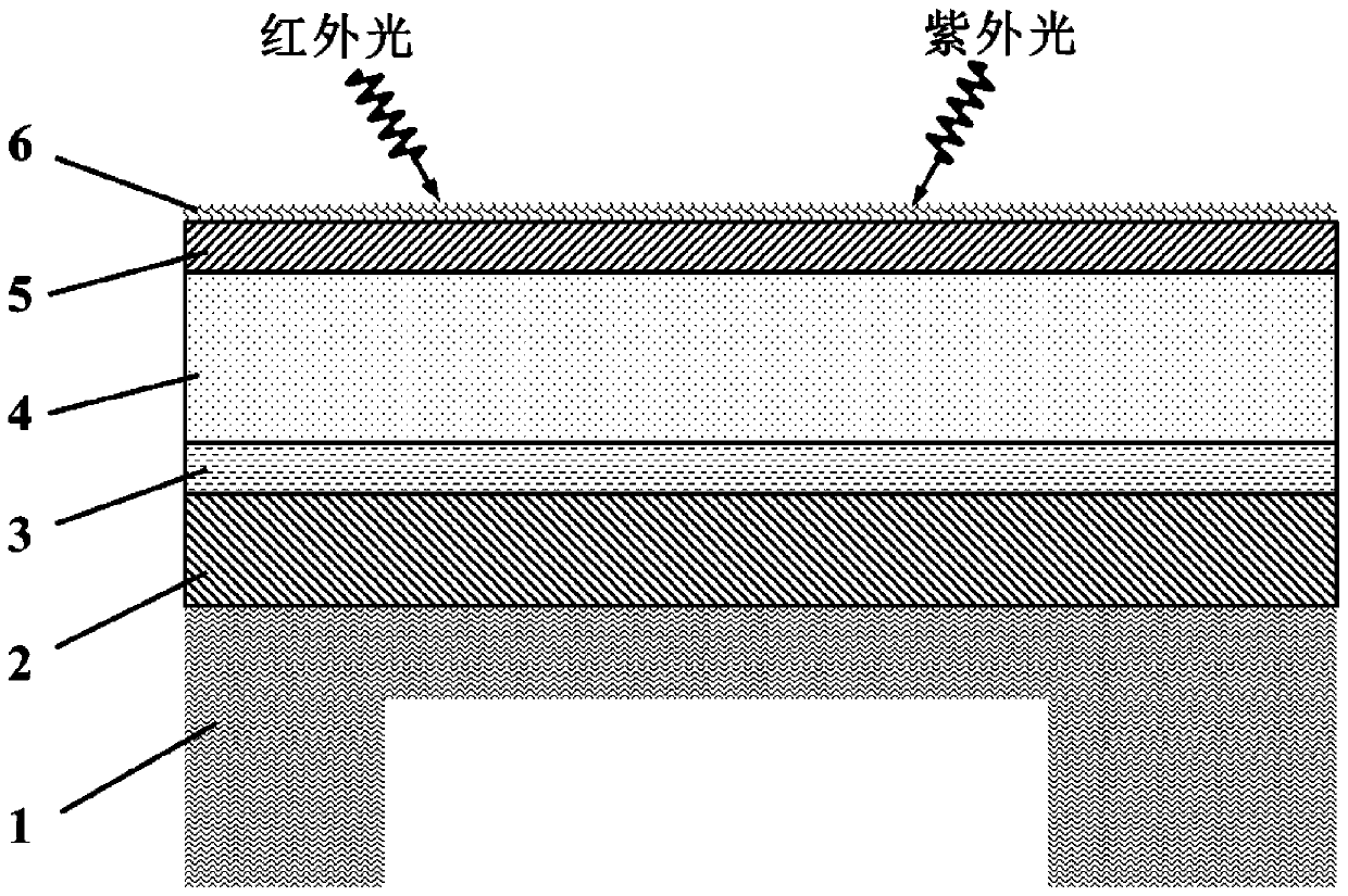
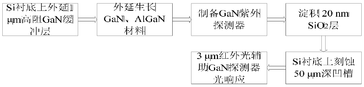
[0033] This implementation case provides a method for increasing the optical switching frequency of a GaN ultraviolet detector. The profile of the device is as follows figure 2 As shown, it consists of Si substrate 1, GaN buffer layer 2, n-type doped GaN layer 3, intrinsically doped GaN layer 4, p-type doped AlGaN layer 5 and SiO 2 Nanoparticles 6 Composition.

[0034] Such as image 3 As shown, the methods include:

[0035] 1) Sampling the substrate and pretreating its surface, and epitaxially growing a 1 μm high-resistance GaN buffer layer 2 on the substrate;

[0036] 2) On the high-resistance GaN buffer layer 2, epitaxially grow an n-type doped GaN layer, an intrinsic doped GaN layer and a p-type doped AlGaN layer in sequence to form an epitaxial layer;

[0037] 3) Patterning the epitaxial layer by photolithography, etching and other processes;

[0038] 4) Deposit 20nm thick SiO on the patterned epitaxial layer 2 nanoparticle layer 6;

[0039] 5) On the Si substrate ...

Embodiment 2

[0042] This implementation case provides a method to increase the optical switching frequency of GaN ultraviolet detectors. The specific preparation process is as follows Figure 4 shown, including:

[0043] 1) Sampling the substrate and pre-treating its surface, and epitaxially growing a 2 μm high-resistance GaN buffer layer 2 on the substrate;

[0044] 2) On the high-resistance GaN buffer layer 2, epitaxially grow an n-type doped GaN layer, an intrinsic doped GaN layer and a p-type doped AlGaN layer in sequence to form an epitaxial layer;

[0045] 3) Patterning the epitaxial layer by photolithography, etching and other processes;

[0046] 4) Deposit 80nm thick SiO on the patterned epitaxial layer 2 nanoparticle layer 6;

[0047] 5) On the Si substrate 1, selectively etch to prepare a thermal insulation groove, the groove depth is 150 μm;

[0048] 6) When detecting or testing ultraviolet light, use infrared light with a wavelength of 3.5 μm to irradiate the photosensitive...

Embodiment 3

[0050] The specific preparation process is as Figure 5 shown, including:

[0051] 1) The substrate is sampled and its surface is pretreated, and a 3 μm high-resistance GaN buffer layer 2 is epitaxially grown on the substrate.

[0052] 2) On the high-resistance GaN buffer layer 2, epitaxially grow an n-type doped GaN layer, an intrinsic doped GaN layer and a p-type doped AlGaN layer in sequence to form an epitaxial layer;

[0053] 3) Patterning the epitaxial layer by photolithography, etching and other processes;

[0054] 4) Deposit 180nm thick SiO on the patterned epitaxial layer 2 nanoparticle layer 6;

[0055] 5) On the Si substrate 1, selectively etch to prepare heat-insulating grooves, the depth of which is 250 μm;

[0056] 6) When detecting or testing ultraviolet light, use infrared light with a wavelength of 4.0 μm to illuminate the photosensitive surface of the GaN detector to assist in photoresponse testing.


PUM

PropertyMeasurementUnit
thicknessaaaaaaaaaa
thicknessaaaaaaaaaa
depthaaaaaaaaaa

Abstract

The invention discloses a method for improving the optical switching frequency of a GaN ultraviolet detector. The method comprises the following steps: 1) growing an epitaxial layer on a Si substrate;2) depositing SiO2 nanoparticles on the detector; 3) etching the bottom of the Si substrate to form a groove; 4) and performing infrared radiation on detector. The detector is heated by infrared irradiation when detecting ultraviolet light to assist the response test of the optical switch. Firstly, the effects of thermal excitation and infrared excitation of carriers are utilized to reduce the capture probability of the trap center to the photo-generated carriers and accelerate the direct transition recombination of the photo-generated carriers so as to improve the optical response speed of the detector; and secondly, the method can be applied to photovoltaic GaN ultraviolet detectors with various structures and is helpful for the detectors to realize fast and high-sensitivity ultravioletdetection.

Description

technical field [0001] The invention relates to the field of ultraviolet detection, in particular to a method for increasing the optical switching frequency of a GaN ultraviolet detector. Background technique [0002] GaN is one of the third-generation wide-bandgap semiconductor materials, with a bandgap as high as 3.4eV. It is the core material for the development of blue lasers and ultraviolet detectors, and is very suitable for highly integrated electronic devices and optoelectronic devices. However, due to the existence of defect levels in the material, such as figure 1 As shown in a, in the GaN ultraviolet detector, some of the photogenerated carriers formed by the excitation of ultraviolet light will be trapped by the center of the trap, resulting in that when the ultraviolet light is turned off, the carriers trapped in the trap cannot be recombined immediately and quickly return to the light previous state. Apparently, the existence of the trapping center will cause...

Claims


Application Information

Patent Timeline
Patent Type & Authority Applications(China)
IPC IPC(8): H01L31/0216H01L31/0236H01L31/0352H01L31/105H01L31/18B82Y30/00
CPCH01L31/02363H01L31/02161H01L31/035281H01L31/105H01L31/1848B82Y30/00Y02E10/544Y02P70/50
Inventor 仇志军叶怀宇张国旗
Owner SOUTH UNIVERSITY OF SCIENCE AND TECHNOLOGY OF CHINA
Why Eureka
Try Eureka