Semiconductor structure and forming method thereof

A semiconductor and graphics technology, applied in the fields of semiconductor devices, semiconductor/solid-state device manufacturing, transistors, etc., can solve the problems of device performance and performance uniformity that need to be improved

Active Publication Date: 2020-01-31
SEMICONDUCTOR MANUFACTURING INTERNATIONAL (BEIJING) CORP +1
View PDF6 Cites 5 Cited by
  • Summary
  • Abstract
  • Description
  • Claims
  • Application Information

AI Technical Summary

Problems solved by technology

[0004] However, after adopting the self-aligned quadruple patterning method, the device performance and performance uniformity still need to be improved

Method used


Image

  • Semiconductor structure and forming method thereof
  • Semiconductor structure and forming method thereof
  • Semiconductor structure and forming method thereof

Examples


Embodiment Construction

[0017] It can be seen from the background art that after adopting the self-aligned quadruple patterning method, the performance of the device still needs to be improved. The reason why the performance of the device needs to be improved is analyzed in combination with a method of forming a semiconductor structure.

[0018] refer to Figure 1 to Figure 6 , shows a structural schematic diagram corresponding to each step in a method for forming a semiconductor structure.

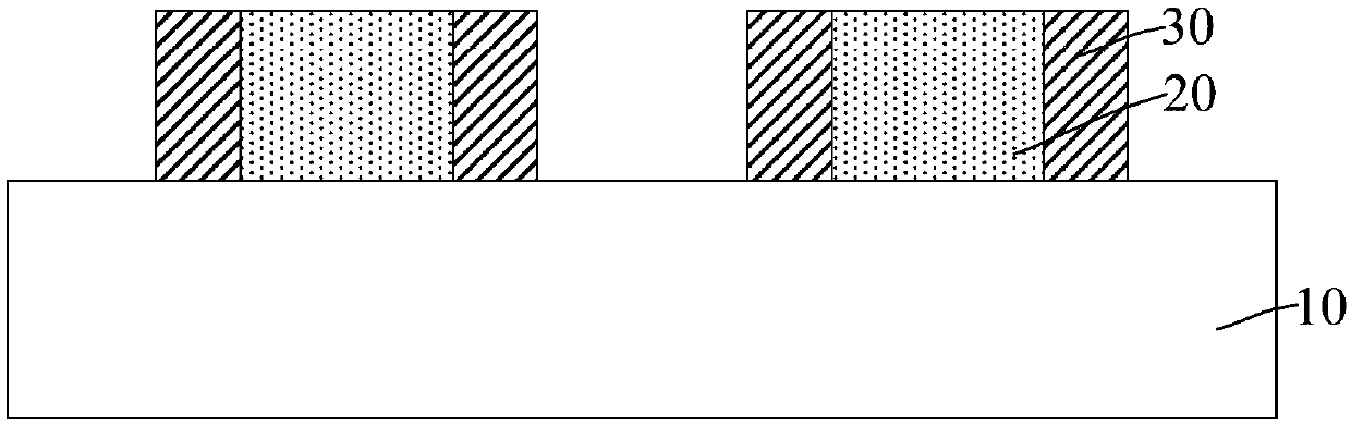
[0019] refer to figure 1 , providing a substrate 10; forming several discrete core layers 20 on the substrate 10; forming sacrificial sidewalls 30 on the sidewalls of the core layer 20.

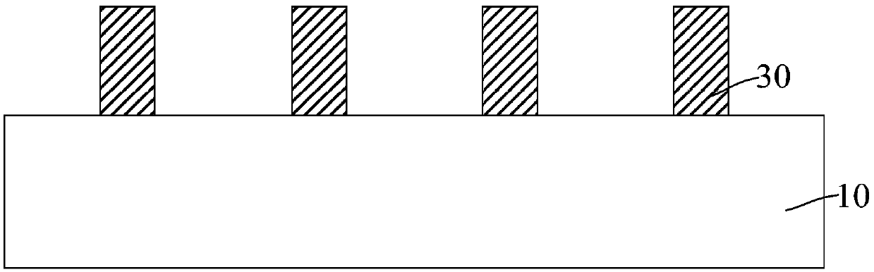
[0020] refer to figure 2 , after forming the sacrificial sidewall 30, remove the core layer 20 (such as figure 1 shown).

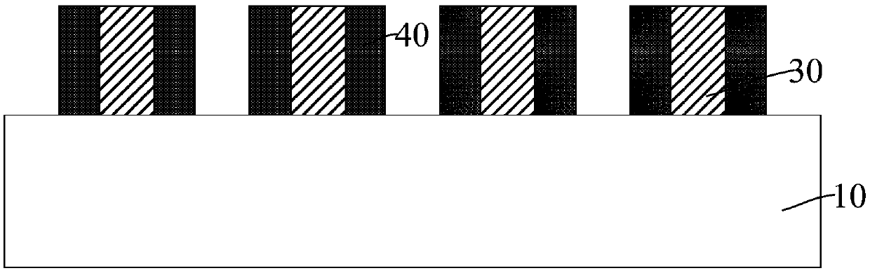
[0021] refer to image 3 , remove the core layer 20 (such as figure 1 As shown), a mask spacer 40 is formed on the sidewall of the sacrificial spacer 30 .

[0022] refer to Figure 4 , after for...


PUM


Abstract

The invention provides a semiconductor structure and a forming method thereof. The forming method comprises the steps that a substrate is provided; a number of discrete core layers are formed on the substrate; sacrificial side walls are formed on the side walls of the core layers; each sacrificial side wall on one side of a core layer is a first sacrificial side wall, and each sacrificial side wall on the other side of the core layer is a second sacrificial side wall; the first sacrificial side walls and the second sacrificial side walls are spaced apart; a first mask side wall is formed on the side wall of each first sacrificial side wall; the core layers are removed, and openings are formed in the sacrificial side walls; a second mask side wall is formed on the side wall, which is exposed by an opening, of each second sacrificial side wall; the sacrificial side walls are removed; and the first mask side walls and the second mask side walls are used as masks to etch the substrate to form a target pattern. According to the invention, the process difficulty of a photolithography process is reduced; the process operability is improved; the shape and size of a target pattern can meetthe process requirements; and the device performance and the performance uniformity are improved.

Description

technical field [0001] The invention relates to the field of semiconductor manufacturing, in particular to a semiconductor structure and a forming method thereof. Background technique [0002] Photolithography (photolithography) technology is a commonly used patterning method and is the most critical production technology in the semiconductor manufacturing process. With the continuous reduction of semiconductor process nodes, the self-aligned double patterning (self-aligned double patterning, SADP) method has become a patterning method favored in recent years, which can increase the density of the pattern formed on the substrate. The density further reduces the pitch between two adjacent patterns, so that the lithography process can overcome the limit of lithography resolution. [0003] With the shrinking of the critical dimension (CD), the self-aligned quadruple patterning (SAQP) method emerges at the historic moment. The density of the pattern formed on the substrate by ...

Claims


Application Information

Patent Timeline
Patent Type & Authority Applications(China)
IPC IPC(8): H01L21/033H01L21/308H01L27/11
CPCH01L21/0337H01L21/3086H10B10/12H01L29/6681H01L21/823821H01L27/0924H01L21/0332H01L21/31053H01L21/31144
Inventor 王楠
Owner SEMICONDUCTOR MANUFACTURING INTERNATIONAL (BEIJING) CORP
Why Eureka
Try Eureka