Dual-current bias type CMOS (Complementary Metal Oxide Semiconductor) pseudo resistor

A pseudo-resistance, dual-current technology, applied in the field of microelectronics, can solve problems such as poor stability, and achieve the effect of avoiding resistance changes and achieving good robustness.

Pending Publication Date: 2020-02-04
XIDIAN UNIV
View PDF1 Cites 6 Cited by
  • Summary
  • Abstract
  • Description
  • Claims
  • Application Information

AI Technical Summary

Problems solved by technology

[0004] However, the resistance value of the small-signal equivalent resistance of the traditional pseudo-re...

Method used


Image

  • Dual-current bias type CMOS (Complementary Metal Oxide Semiconductor) pseudo resistor
  • Dual-current bias type CMOS (Complementary Metal Oxide Semiconductor) pseudo resistor
  • Dual-current bias type CMOS (Complementary Metal Oxide Semiconductor) pseudo resistor

Examples


Embodiment 1

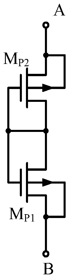
[0031] See figure 1 , figure 1 is a schematic diagram of the structure of a traditional pseudo-resistor, as shown in the figure, the traditional pseudo-resistor includes two PMOS field effect transistors M P1 and M P2 , the A terminal and the B terminal are respectively used as the two ends of the pseudo-resistor, and the connection method is shown in figure 1 , the small-signal equivalent resistance value of the traditional pseudo-resistor is deduced as follows.

[0032] Based on the EKV transistor model, the I-V relationship of the PMOS transistor is as follows:

[0033]

[0034] Among them, n p Indicates the subthreshold slope factor of the PMOS tube, μ P Indicates the hole mobility of the PMOS tube, V TH Indicates the threshold voltage of the PMOS tube, C ox Indicates the capacitance of the gate oxide layer of the PMOS transistor, W / L indicates the ratio of the channel width to the channel length of the PMOS transistor, V T Indicates temperature voltage, V BG I...

Embodiment 2

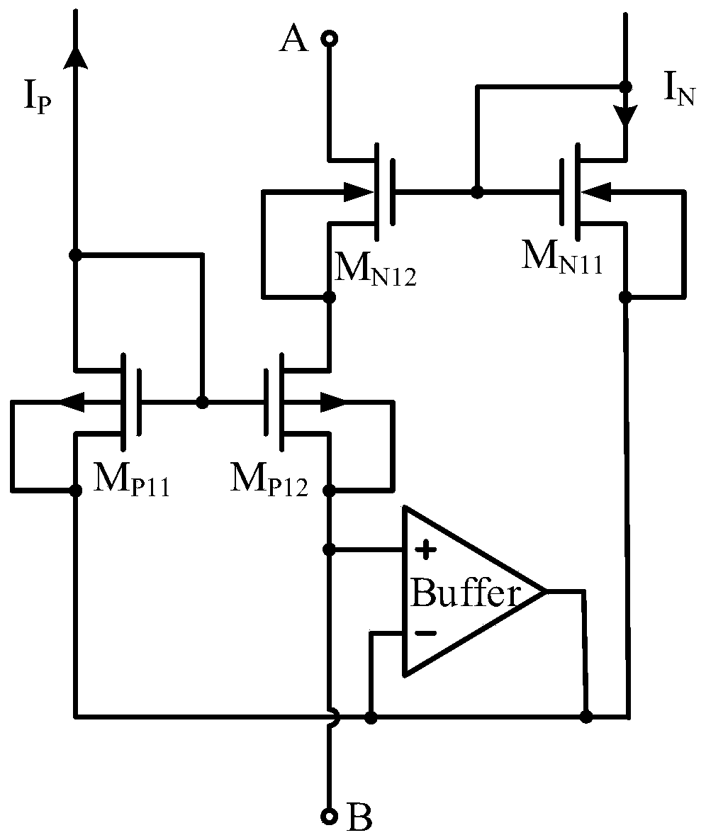
[0061] This embodiment provides a dual-current biased CMOS pseudo-resistor circuit, including a current source unit and a number of dual-current-biased CMOS pseudo-resistors in series as described in Embodiment 1, wherein the current source unit is coupled to The first PMOS transistor M connected to several CMOS pseudo-resistors connected in series with double current bias P11 The drain and the first NMOS transistor M N11 The drain is used to provide a bias current proportional to the absolute temperature; the adjacent series-connected double-current-biased CMOS pseudo-resistors share a buffer Buffer.

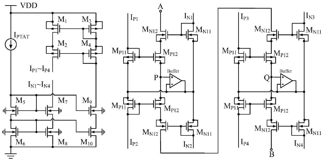
[0062] See image 3 , image 3 It is a schematic diagram of a dual current biased CMOS pseudo-resistor circuit provided by an embodiment of the present invention. In this embodiment, four CMOS pseudo-resistors with dual current bias are connected in series, and the current source unit includes a current source I PTAT , the first MOS tube M 1 , the second MOS tube M 2 , th...

Embodiment 3

[0071] This embodiment provides another double-current biased CMOS pseudo-resistor circuit. Compared with Embodiment 2, the dual-current-biased CMOS pseudo-resistor in this embodiment is connected in parallel, and the current source unit is the same as that in Embodiment 2. The structures are the same, and the drains of the first PMOS transistor and the drains of the first NMOS transistors of the plurality of double-current-biased CMOS pseudo-resistors connected in parallel are used to provide a bias current proportional to the absolute temperature.

[0072] See Figure 4 , Figure 4 is a schematic diagram of another dual current biased CMOS pseudo-resistor circuit provided by an embodiment of the present invention. In this embodiment, two dual-current biased CMOS pseudo-resistors are connected in parallel, and the second MOS transistor M 2 The drains are respectively connected to the first PMOS transistor M of two double current biased CMOS pseudo-resistors P11 The drain o...


PUM


Abstract

The invention relates to a dual-current bias type CMOS (Complementary Metal Oxide Semiconductor) pseudo resistor, which comprises a first PMOS transistor, a second PMOS transistor, a first NMOS transistor, a second NMOS transistor and a buffer. The drain electrode of the first PMOS transistor is connected with the grid electrode of the first PMOS transistor. A substrate is connected with the source electrode of the first PMOS transistor, the grid electrode is connected with the grid electrode of the second PMOS transistor, and the source electrode is connected with the source electrode of thefirst NMOS transistor; the substrate of the second PMOS transistor is connected with the source electrode of the second PMOS transistor, the drain electrode of the second PMOS transistor is connectedwith the source electrode of the second NMOS transistor, and the source electrode serves as the first end of the CMOS pseudo resistor; the drain of the first NMOS transistor is connected with the grid of the first NMOS transistor, the substrate is connected with the source of the first NMOS transistor, and the grid is connected with the grid of the second NMOS transistor; the substrate of the second NMOS transistor is connected with the source of the second NMOS transistor, and the drain of the second NMOS transistor is used as the second end of the CMOS pseudo resistor; the non-inverting input end of the buffer is connected with the source electrode of the second PMOS tube, the inverting input end of the buffer is connected with the source electrode of the first PMOS tube, and the outputend of the buffer is connected with the source electrode of the first NMOS tube. The resistance value of the dual-current bias CMOS pseudo resistor is basically not affected by the process, temperature change and sub-threshold leakage current, and the robustness is good.

Description

technical field [0001] The invention belongs to the technical field of microelectronics, and in particular relates to a CMOS pseudo-resistor with double current bias. Background technique [0002] Under the condition of MOS technology, it needs to occupy a large chip area to make a resistor with a large resistance value (GΩ order). Pseudo-resistors composed of effect transistors are often used to replace traditional resistors. [0003] Traditional pseudoresistive structures such as figure 1 As shown, it includes two diode-connected PMOS field effect transistors, that is, a PMOS field effect transistor whose gate and drain are short-circuited. The diode-connected MOS field-effect transistor device has a very large equivalent small-signal resistance, and two diode-connected PMOS field-effect transistors are connected back to back to form a traditional pseudo-resistive structure. The traditional pseudo-resistor structure has a very large equivalent small-signal resistance, a...

Claims


Application Information

Patent Timeline
IPC IPC(8): H03H11/46
CPCH03H11/53
Inventor 刘帘曦陈明仑华天源张怡朱樟明
Owner XIDIAN UNIV
Why Eureka
Try Eureka