Sealing cover high-thermal-conductivity packaging structure for sorted flip chips and packaging process thereof

A technology of flip-chip and packaging structure, which is applied in the direction of semiconductor devices, semiconductor/solid-state device manufacturing, semiconductor/solid-state device components, etc., and can solve problems such as inability to meet individual requirements

Inactive Publication Date: 2020-02-07
太极半导体(苏州)有限公司
View PDF8 Cites 1 Cited by
  • Summary
  • Abstract
  • Description
  • Claims
  • Application Information

AI Technical Summary

Problems solved by technology

[0003] However, when the thickness of the sorting flip chip is less than 500 μm, and the cavity depth of the conventional metal cover is higher than 800 μm, the thermal paste on the normal brush interface cannot completely fill the minimum gap space of about 300 μm or even larger, and achieve efficient heat dissipation; thus only Plastic packaging (EMC) type FCBGA packaging can be used, which cannot meet the individual requirements of customers for the packaging form; especially on the premise that the metal cover shares the mold and the size is unified to ensure that the cost is minimized

Method used


Image

  • Sealing cover high-thermal-conductivity packaging structure for sorted flip chips and packaging process thereof
  • Sealing cover high-thermal-conductivity packaging structure for sorted flip chips and packaging process thereof
  • Sealing cover high-thermal-conductivity packaging structure for sorted flip chips and packaging process thereof

Examples


Embodiment Construction

[0043] The present invention is described below in conjunction with accompanying drawing.

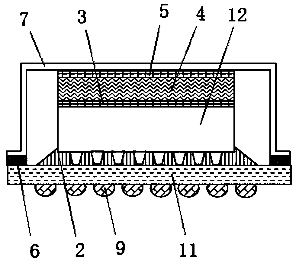
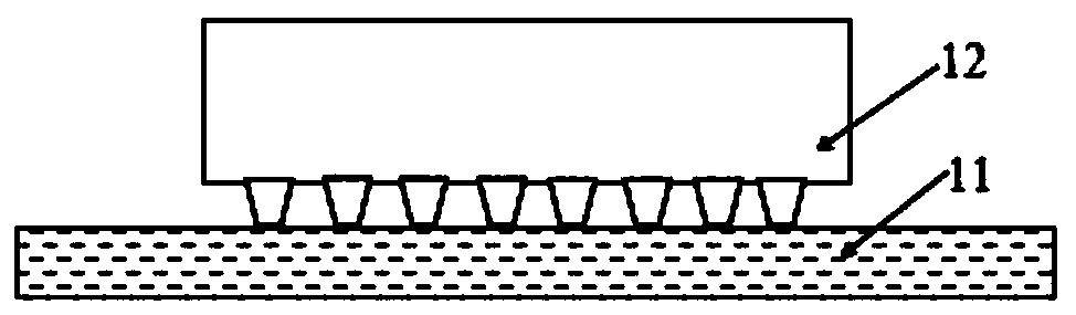
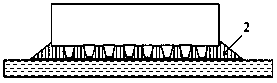
[0044] as attached figure 1 As shown, a kind of capping high thermal conductivity packaging structure for sorting flip chips according to the present invention includes a substrate 11, a flip chip 12 and a metal cover 7, the bottom of the substrate 11 is soldered with solder balls 9, and the metal cover 7 The frame is welded on the substrate 11 by solder 6, and the flip chip 12 is located in the metal cover 7; the front side of the flip chip 12 has a plurality of bumps, and a filling glue 2 is arranged between the flip chip 12 and the substrate 11, and the filling The glue 2 fills the gap between the flip chip 12 and the substrate 11, and the gap between the bumps; the other side of the flip chip 12 is provided with a nickel-plated copper sheet 4, and the nickel-plated copper sheet 4 passes through The lower thermally conductive adhesive layer 3 on the lower side is pasted on the back ...


PUM

PropertyMeasurementUnit
thicknessaaaaaaaaaa

Abstract

The invention discloses a sealing cover high-thermal-conductivity packaging structure for sorted flip chips and a packaging process thereof. The sealing cover high-thermal-conductivity packaging structure comprises a substrate, a flip chip, a metal cover and a nickel-plated copper sheet. The metal cover is welded on the substrate, and the flip chip is located in the metal cover. Filling glue is arranged between the flip chip and the substrate. The nickel-plated copper sheet is pasted on the back surface of the flip chip through a lower heat conduction adhesive layer. The nickel-plated copper sheet is bonded with the metal cover through an upper heat conduction adhesive layer. According to the scheme, the structure in which the upper and lower heat conduction adhesive layers and the nickel-plated copper sheet are combined is adopted, and high-thermal-conductivity sealing cover product packaging is achieved. The nickel-plated copper sheet is low in manufacturing cost and high in practicability, and the heat conduction coefficient of the nickel-plated copper sheet is about 2.6 times that of a silicon gasket. Rapid transfer of heat from the thin sorted flip chip to the metal cover is realized, personalized pursuit of clients for packaging types is satisfied, the packaging structure is suitable for a larger gap between the chip and the metal cover and a higher heat dissipation requirement, and the process also has higher mass production operability.

Description

technical field [0001] The invention relates to a capping high thermal conductivity packaging structure for sorting flip-chips and a packaging process thereof, belonging to the technical field of integrated circuit flip-chip packaging. Background technique [0002] When the chip is flip-chip soldered on a substrate or other carrier board, it is generally necessary to embed an underfiller between the bumps of the chip, and the bottom of the metal cover (Lid cover) is strongly connected to the substrate by an adhesive. The substrate or other carrier is supported; the top of the cavity of the metal cover is connected to the back of the chip (non-electrical surface) through the interface heat dissipation material (TIM glue) to realize heat conduction, and then the ball is planted and cut into shape. [0003] However, when the thickness of the sorting flip chip is less than 500 μm, and the cavity depth of the conventional metal cover is higher than 800 μm, the thermal paste on th...

Claims


Application Information

Patent Timeline
Patent Type & Authority Applications(China)
IPC IPC(8): H01L23/31H01L23/367H01L21/56H01L21/48
CPCH01L21/4882H01L21/56H01L23/3128H01L23/3672H01L2224/16225H01L2224/32225H01L2224/73204H01L2224/73253H01L2924/15311H01L2924/00
Inventor 阳芳芳汪婷马军张光明
Owner 太极半导体(苏州)有限公司
Why Eureka
Try Eureka