LED containing PMOT:PPV/ZnO:Cu/ZnO:Al heterojunction and preparation method thereof

A heterojunction and polycrystalline layer technology, which is applied in the manufacture of semiconductor/solid-state devices, electrical components, circuits, etc., can solve the problems of limited value of photobiological effects, and achieve the effects of low equipment and raw material prices, simple and safe methods and processes.

Active Publication Date: 2020-02-11
CHANGAN UNIV
View PDF5 Cites 0 Cited by
  • Summary
  • Abstract
  • Description
  • Claims
  • Application Information

AI Technical Summary

Problems solved by technology

[0003] Aiming at the defects and insufficiencies of the existing preparation technology, the present invention provides an LED containing PMOT:PPV/ZnO:Cu/ZnO:Al heterojunction and its preparation method, which

Method used


Image

  • LED containing PMOT:PPV/ZnO:Cu/ZnO:Al heterojunction and preparation method thereof
  • LED containing PMOT:PPV/ZnO:Cu/ZnO:Al heterojunction and preparation method thereof

Examples


Embodiment 1

[0032] Following the above technical scheme and in conjunction with the accompanying drawings, this embodiment provides a method for preparing an LED containing PMOT:PPV / ZnO:Cu / ZnO:Al heterojunction, including the following steps:

[0033] Step 1: Put the ITO substrate into the magnetron sputtering vacuum chamber, use 99.99% zinc target and 99.9% aluminum target, pass in 3pa oxygen and 2pa argon, control the temperature of the substrate to 300°C, and use 110W power Co-sputtering was carried out for 30 min under the ITO substrate, and a ZnO:Al polycrystalline layer was obtained on the ITO substrate, and the samples were taken out. The molar ratio of ZnO to Al is 97:3.

[0034] Step 2: Prepare a mixed solution of zinc acetate and copper nitrate, the concentrations of zinc acetate and copper nitrate are 0.04mol / L and 0.005mol / L respectively, then put the ZnO:Al polycrystalline layer into the mixed solution, and raise the temperature to 95°C, After waiting for its growth for 5 ho...

Embodiment 2

[0038] Embodiment 2 (contrast):

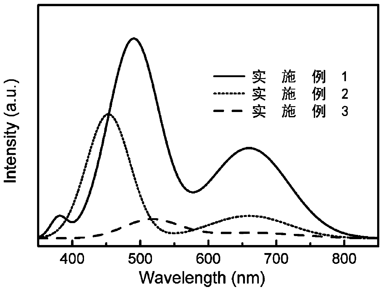
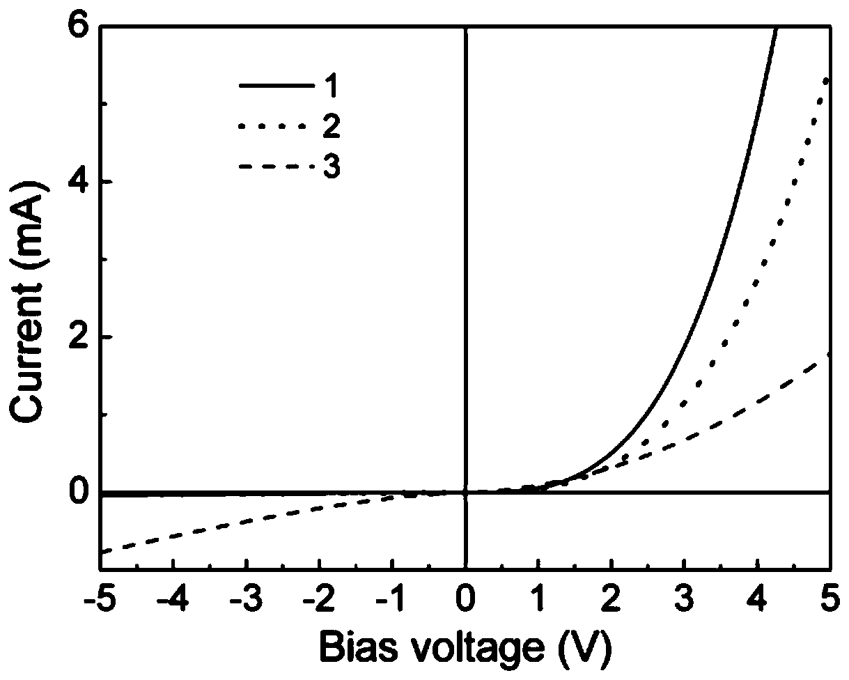
[0039] The preparation method is the same as in Example 1, but step 2 is omitted, and the prepared device is a PMOT:PPV / ZnO:Al heterojunction. From figure 1 It can be seen that the main luminescence peak changes from around 490nm to around 450nm after shifting, indicating that it cannot have the same photobiological enhancement effect as Example 1, and its luminous intensity is obviously weaker than that of Example 1. From figure 2 It can be seen that the forward current is small, the reverse current is large, the rectification ratio is low, the rectification effect of the current-voltage characteristics is not as good as that of Example 1, and the electric injection efficiency is not as good as that of Example 1, because the device energy band structure of Example 2 Not as reasonable as that made in Example 1.

Embodiment 3

[0040] Embodiment 3 (contrast):

[0041] The preparation method and test are the same as in Example 1, but step 4 is omitted. From figure 1 It can be seen that the main peak of the photobiological effect at 490nm is significantly weaker than that of Example 1, and the overall luminous intensity is also significantly weaker than that of Example 1. From figure 2 It can be seen that the forward current is small, the reverse current is large, the rectification ratio is low, the rectification effect of the current-voltage characteristics is not as good as that of Example 1, and the electric injection efficiency is not as good as that of Example 1, because Example 3 has not been treated with plasma. The surface impurities of the PMOT:PPV / ZnO:Cu / ZnO:Al heterojunction LED are more than the surface impurities of the PMOT:PPV / ZnO:Cu / ZnO:Al heterojunction LED treated by plasma in Example 1.


PUM


Abstract

The invention discloses a preparation method for an LED containing a PMOT:PPV/ZnO:Cu/ZnO:Al heterojunction. The method is characterized by comprising the following steps: a ZnO:Cu/ZnO:Al heterojunction grows on an ITO substrate, spin-coating of a mixed solution of PMOT and PPV on the ZnO:Cu polycrystalline layer of the ZnO:Cu/ZnO:Al heterojunction is carried out for heat treatment; and finally, aTi electrode is plated on the ZnO:Cu polycrystalline layer surface. The step of growing the ZnO:Cu/ZnO:Al heterojunction on the ITO substrate comprises substeps: an ZnO:Al polycrystalline layer growson the ITO substrate; the ZnO:Al polycrystalline layer is then put into a mixed solution of zinc acetate and copper nitrate; a ZnO:Cu polycrystalline layer grows on the surface of the ZnO:Al polycrystalline layer; and finally, the ZnO:Cu/ZnO:Al heterojunction is obtained on the ITO substrate. Through spectral modulation based on semiconductor energy band engineering, a main luminescence peak of 490nm is realized, and a more excellent photobiological effect can be provided. The preparation method disclosed by the invention is simple and safe in process, low in price of used equipment and raw materials and suitable for industrial large-scale preparation.

Description

technical field [0001] The invention belongs to the field of electronic materials and preparation thereof, in particular to an LED containing PMOT:PPV / ZnO:Cu / ZnO:Al heterojunction and a preparation method thereof. Background technique [0002] LED is a semiconductor light-emitting diode. LED has the characteristics of energy saving, environmental protection, long life and small size. It can be widely used in various indications, displays, decorations, backlights, general lighting and urban night scenes. Semiconductor ZnO nanowires have been successfully assembled into different types of nanodevices, such as nanowire field-effect transistors, nanowire lasers, nanowire sensors, and nanowire LEDs. However, some existing devices have unstable luminous performance and high working voltage. Research on UV LEDs based on ZnO nanorods has not been very successful, and its electroluminescence is basically in the visible light band. The main luminous peak of commercial gallium nitrid...

Claims


Application Information

Patent Timeline
IPC IPC(8): H01L51/50H01L51/54H01L51/56
CPCH10K85/113H10K50/00H10K71/00
Inventor 段理魏星郭婷婷王昭
Owner CHANGAN UNIV
Why Eureka
Try Eureka