Semiconductor device and forming method thereof

A semiconductor and device technology, applied in the field of semiconductor devices and their formation, can solve the problems of easy leakage, low ion concentration, and inability to meet the normal function of the device, and achieve the effect of ensuring current isolation and leakage.

Active Publication Date: 2020-02-25
SEMICON MFG INT (SHANGHAI) CORP +1
View PDF5 Cites 2 Cited by
  • Summary
  • Abstract
  • Description
  • Claims
  • Application Information

AI Technical Summary

Problems solved by technology

If the width of the channel is narrowed, the short channel effect (SCE) appears, and the normal function of the device cannot be satisfied.
[0003] At present, the source / drain on both sides of the channel is doped with ions, but due to the technical characteristics of doping, the ion concentration in the source / drain is not uniform, and the ion concentration in the lower part of the source / drain is lower than that in the upper part, and Ion concentrations are lower in the lower part of the source / drain near the channel
When a voltage is applied, it is easy to leak electricity, which reduces the performance of semiconductor devices

Method used


Image

  • Semiconductor device and forming method thereof
  • Semiconductor device and forming method thereof
  • Semiconductor device and forming method thereof

Examples


Embodiment Construction

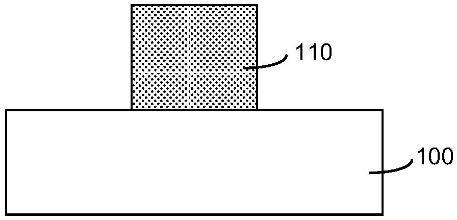
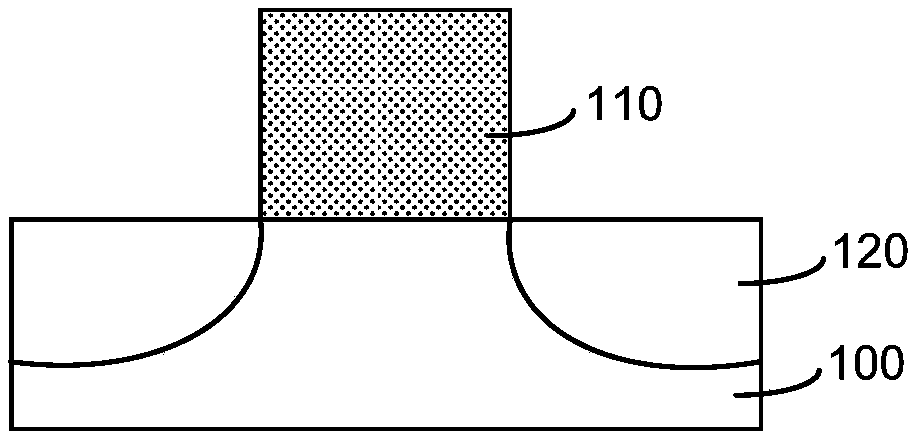
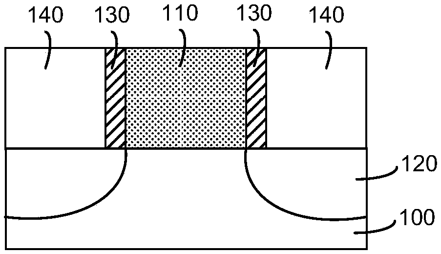
[0031] As mentioned above, in the existing semiconductor devices, there is a problem that the current is easy to leak in the source / drain and the lower part of the channel.

[0032] After research, it is found that the reason for the above problems is that the ion concentration in the lower part of the source / drain is lower than that in the upper part, and the impurity ions in the lower part of the source / drain are easy to diffuse into the channel to form an impurity diffusion region. When a voltage is applied, a current flows between the magazine diffusion regions, causing leakage and reducing the performance of the semiconductor device.

[0033] In order to solve this problem, the present invention provides a method for forming a semiconductor device. A diffusion barrier structure is formed between the lower part of the source / drain and the lower part of the channel, which can effectively avoid leakage and improve the performance of the device.

[0034] Various exemplary emb...


PUM

PropertyMeasurementUnit
widthaaaaaaaaaa

Abstract

The invention discloses a forming method of a semiconductor device. The method comprises the following steps of: providing a semiconductor substrate and a gate structure which is formed on the semiconductor substrate; etching the semiconductor substrate on two sides of the gate structure to form a first groove; forming a source/drain in the first groove, wherein an area under the gate structure and between the source/drain is a channel; etching part of the source/drain or part of the semiconductor substrate to form a second groove, wherein the second groove is adjacent to one side, close to the gate structure, of the remaining source/drain; forming a diffusion barrier structure at the bottom of the second groove, wherein the ion type in the diffusion barrier structure is opposite to the ion type in the source/drain, the top of the diffusion barrier structure is higher than the bottom of the source/drain, and the bottom of the diffusion barrier structure is not higher than the bottom ofthe source/drain; and forming a dielectric layer in the second groove. The diffusion barrier structure can effectively avoid current leakage at the lower part of the channel and the lower part of thesource/drain, avoid electric leakage and improve the performance of the semiconductor device.

Description

technical field [0001] The invention relates to the field of semiconductor manufacturing, in particular to a semiconductor device and a forming method thereof. Background technique [0002] With the improvement of the integration level of semiconductor devices, the size of the devices is gradually reduced, and the size of key structures is also reduced accordingly. If the width of the channel is narrowed, the short channel effect (SCE) appears, and the normal function of the device cannot be satisfied. [0003] At present, the source / drain on both sides of the channel is doped with ions, but due to the technical characteristics of doping, the ion concentration in the source / drain is not uniform, and the ion concentration in the lower part of the source / drain is lower than that in the upper part, and In the lower part of the source / drain near the channel, the ion concentration is lower. When a voltage is applied, it is easy to leak electricity, which reduces the performance...

Claims


Application Information

Patent Timeline
Patent Type & Authority Applications(China)
IPC IPC(8): H01L21/336H01L29/78H01L29/06
CPCH01L29/78H01L29/66568H01L29/0603
Inventor 赵猛
Owner SEMICON MFG INT (SHANGHAI) CORP
Why Eureka
Try Eureka